
Intel 945P Motherboards: Going from Hopeless to Enthusiastic
- Posted in
- Motherboards
EPOX 5LDA+GLI: Features
The Intel ICH7R IDE port connector is located near the edge of the board and did not present any connection issues in our mid-size ATX case.
The Intel SATA II ports are conveniently located below the ICH7R chipset and above the primary IDE connector. The SATA II ports feature the new clamp and latch design. Epox did not include the new cable designs in their accessory kit, which greatly enhance the security of the SATA connections.
The floppy drive port connector is placed along the bottom left edge of the board and could create cable management issues in tower cases. The CP80P post port debug LED and BIOS chip are located to the right of the floppy drive connector. The additional power on and reset buttons are located in between the BIOS chip and the Intel SATA II ports.
The Intel USB connectors, IEEE1394a connectors, and Com2 serial port are located along the left edge of the board and are a tight fit when utilizing the bottom PCI slot. The CMOS reset is a traditional jumper design located to the left of the Intel ICHR7 chipset.
In between the two x16 PCI Express slots is the single x1 PCI Express slot. This configuration could potentially render this slot useless when utilizing the first x16 PCI Express slot. We did not have any issues utilizing this slot with video cards containing single slot cooling systems, yet we were unable to install a network card upon installation of a NVIDIA 6800 Ultra in the x16 PCI Express slot. Regardless, the layout of this area is organized better than the Asus P5LD2 Deluxe.
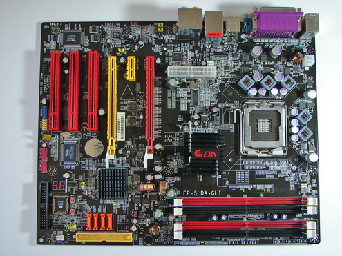
The Northbridge and Southbridge chipsets are passively cooled with heatsinks that do not interfere with any installed peripherals. In fact, this system kept the chipsets cool enough that additional chipset voltage was not a factor in our overclocking tests. Epox places the four-pin 12V auxiliary power connector at the top of the CPU socket area, but out of the way of most aftermarket cooling solutions. The five-phase switching power design is visible in this picture.
The BIOS options are acceptable on the 5LDA+GLI, with memory voltage to 2.15V, and a wide range of chipset, bus, and vCore voltage adjustments. Memory ratios are limited compared to the nForce4 Intel Edition boards, but Epox did provide a variety of settings. The board fully supports manual memory timing adjustments or allows for an Auto setting that will set the memory to the SPD settings. This Auto setting will adjust the memory timing settings automatically when the system is overclocked.
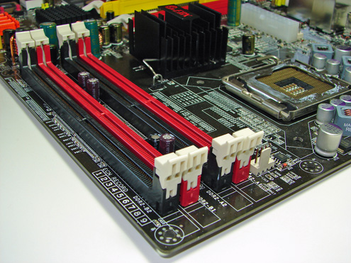
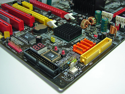
The Intel ICH7R IDE port connector is located near the edge of the board and did not present any connection issues in our mid-size ATX case.
The Intel SATA II ports are conveniently located below the ICH7R chipset and above the primary IDE connector. The SATA II ports feature the new clamp and latch design. Epox did not include the new cable designs in their accessory kit, which greatly enhance the security of the SATA connections.
The floppy drive port connector is placed along the bottom left edge of the board and could create cable management issues in tower cases. The CP80P post port debug LED and BIOS chip are located to the right of the floppy drive connector. The additional power on and reset buttons are located in between the BIOS chip and the Intel SATA II ports.
The Intel USB connectors, IEEE1394a connectors, and Com2 serial port are located along the left edge of the board and are a tight fit when utilizing the bottom PCI slot. The CMOS reset is a traditional jumper design located to the left of the Intel ICHR7 chipset.
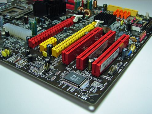
In between the two x16 PCI Express slots is the single x1 PCI Express slot. This configuration could potentially render this slot useless when utilizing the first x16 PCI Express slot. We did not have any issues utilizing this slot with video cards containing single slot cooling systems, yet we were unable to install a network card upon installation of a NVIDIA 6800 Ultra in the x16 PCI Express slot. Regardless, the layout of this area is organized better than the Asus P5LD2 Deluxe.
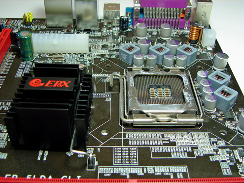
The Northbridge and Southbridge chipsets are passively cooled with heatsinks that do not interfere with any installed peripherals. In fact, this system kept the chipsets cool enough that additional chipset voltage was not a factor in our overclocking tests. Epox places the four-pin 12V auxiliary power connector at the top of the CPU socket area, but out of the way of most aftermarket cooling solutions. The five-phase switching power design is visible in this picture.
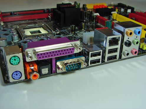
The BIOS options are acceptable on the 5LDA+GLI, with memory voltage to 2.15V, and a wide range of chipset, bus, and vCore voltage adjustments. Memory ratios are limited compared to the nForce4 Intel Edition boards, but Epox did provide a variety of settings. The board fully supports manual memory timing adjustments or allows for an Auto setting that will set the memory to the SPD settings. This Auto setting will adjust the memory timing settings automatically when the system is overclocked.
Originally published at https://www.anandtech.com/show/1857 (Wayback Machine).