
ASUS Striker II Formula under the Microscope
- Posted in
- Motherboards
To Sync or Not to Sync, that is the Question
One thing that has remained fairly unique to the NVIDIA chipsets is their ability to run the memory bus and FSB asynchronously from one another. In truth, the chipset just selects the nearest available memory divider to what the user inputs into the BIOS memory speed option. Basically, NVIDIA employs a lot of memory dividers and this gives them what appears to be a lot more freedom for overclockers.
For asynchronous memory speeds to work properly, additional tRD offsets must be employed to ensure that bus-to-bus data transfers fall within the timing window set by CAS (Column Address Strobe), the applied divider, and tRD. The result of this is usually a performance penalty, which is especially apparent when there are fewer memory cycles to FSB cycles (using a "down" divider) within a given period. In short, a percentage of the FSB cycles will pass without any data transfer taking place, while the MCH has to wait for a memory cycle to become available. The diagrams below should help us visualize this taking place a little better.
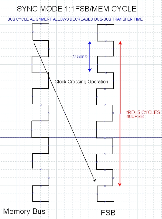
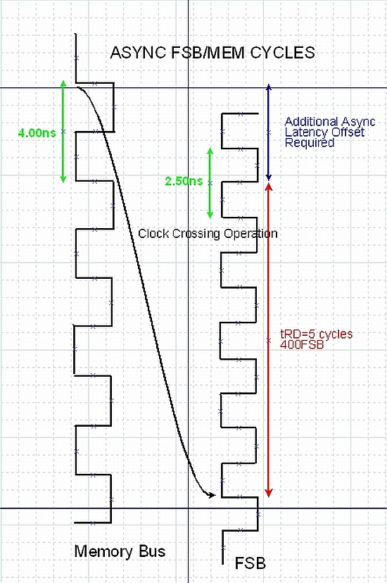
In sync mode, no additional tRD offsets are required, because a memory cycle is always available to the FSB to make a data acquisition. This makes it far easier to predict the rules of which CAS and tRD combinations will work together. However, when we expand this to include a myriad of divider combinations it's no surprise why many users have stumbled across "memory holes" on the 680i chipset that result in the motherboard not booting when certain combinations of timings are used. Users are again encouraged to read this article to obtain an understanding of tRD/memory divider and CAS relationships.
NVIDIA has worked very hard to eradicate these holes, and one of the key ways to employ a failsafe is to prohibit the manual adjustment of tRD via BIOS, rather opting for a static tRD value based upon the FSB speed selected by the end user. This way, the BIOS engineers can predict the possible permutations of memory timing and FSB speeds and ensure that the board is at least able to boot.
Moving on, the use of "up" dividers (where there are more memory cycles than FSB cycles in a give time frame), is not something we consider totally evil, as there are at least enough memory cycles to saturate the FSB with data. It is wise to generally aim for Sync mode wherever possible and at the most use an up divider if necessary. The Striker II generally tops out in Sync mode around 975MHz when overclocking. Of course, 2T timing rates are mandatory for 24/7 use when the memory bus is operating at this speed. 1T command rate is really only available for use below DDR2-850 speeds and requires judicious levels of VMCH to hold stability. 8GB overclocking is obviously bound by the rules of 2T command rates for operation at this time.
Originally published at https://www.anandtech.com/show/2484 (Wayback Machine).