
NVIDIA GeForce GTX 295: Leading the Pack
- Posted in
- GPUs
Now that we have some hardware in our hands and NVIDIA has formally launched the GeForce GTX 295, we are very interested in putting it to the test. NVIDIA's bid to reclaim the halo is quite an interesting one. If you'll remember from our earlier article on the hardware, the GTX 295 is a dual GPU card that features two chips that combine aspects of the GTX 280 and the GTX 260. The expectation should be that this card will fall between GTX 280 SLI and GTX 260 core 216 SLI.
As for the GTX 295, the GPUs have the TPCs (shader hardware) of the GTX 280 with the memory and pixel power of the GTX 260. This hybrid design gives it lots of shader horsepower with less RAM and raw pixel pushing capability than GTX 280 SLI. This baby should perform better than GTX 260 SLI and slower than GTX 280 SLI. Here are the specs:
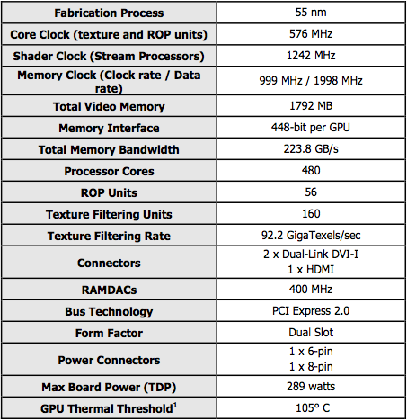
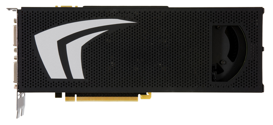
Our card looks the same as the one in the images provided by NVIDIA that we posted in December. It's notable that the GPUs are built at 55nm and are clocked at the speed of a GTX 260 despite having the shader power of the GTX 280 (x2).
We've also got another part coming down the pipe from NVIDIA. The GeForce GTX 285 is a 55nm part that amounts to an overclocked GTX 280. Although we don't have any in house yet, this new card was announced on the 8th and will be available for purchase on the 15th of January 2009.
There isn't much to say on the GeForce GTX 285: it is an overclocked 55nm GTX 280. The clock speeds compare as follows:
| Core Clock Speed (MHz) | Shader Clock Speed (MHz) | Memory Data Rate (MHz) | |
| GTX 280 | 602 | 1296 | 2214 |
| GTX 285 | 648 | 1476 | 2484 |
We don't have performance data for the GTX 285 yet, but expect it (like the GTX 280 and GTX 295) to be necessary only with very large displays.
| GTX 295 | GTX 285 | GTX 280 | GTX 260 Core 216 | GTX 260 | 9800 GTX+ | |
| Stream Processors | 2 x 240 | 240 | 240 | 216 | 192 | 128 |
| Texture Address / Filtering | 2 x 80 / 80 | 80 / 80 | 80 / 80 | 72/72 | 64 / 64 | 64 / 64 |
| ROPs | 28 | 32 | 32 | 28 | 28 | 16 |
| Core Clock | 576MHz | 648MHz | 602MHz | 576MHz | 576MHz | 738MHz |
| Shader Clock | 1242MHz | 1476MHz | 1296MHz | 1242MHz | 1242MHz | 1836MHz |
| Memory Clock | 999MHz | 1242MHz | 1107MHz | 999MHz | 999MHz | 1100MHz |
| Memory Bus Width | 2 x 448-bit | 512-bit | 512-bit | 448-bit | 448-bit | 256-bit |
| Frame Buffer | 2 x 896MB | 1GB | 1GB | 896MB | 896MB | 512MB |
| Transistor Count | 2 x 1.4B | 1.4B | 1.4B | 1.4B | 1.4B | 754M |
| Manufacturing Process | TSMC 55nm | TSMC 55nm | TSMC 65nm | TSMC 65nm | TSMC 65nm | TSMC 55nm |
| Price Point | $500 | $??? | $350 - $400 | $250 - $300 | $250 - $300 | $150 - 200 |
For this article will focus heavily on the performance of the GeForce GTX 295, as we've already covered the basic architecture and specifications. We will recap them and cover the card itself on the next page, but for more detail see our initial article on the subject.
The Test
| Test Setup | |
| CPU | Intel Core i7-965 3.2GHz |
| Motherboard | ASUS Rampage II Extreme X58 |
| Video Cards | ATI Radeon HD 4870 X2 ATI Radeon HD 4870 1GB NVIDIA GeForce GTX 295 NVIDIA GeForce GTX 280 SLI NVIDIA GeForce GTX 260 SLI NVIDIA GeForce GTX 280 NVIDIA GeForce GTX 260 |
| Video Drivers | Catalyst 8.12 hotfix ForceWare 181.20 |
| Hard Drive | Intel X25-M 80GB SSD |
| RAM | 6 x 1GB DDR3-1066 7-7-7-20 |
| Operating System | Windows Vista Ultimate 64-bit SP1 |
| PSU | PC Power & Cooling Turbo Cool 1200W |
Originally published at https://www.anandtech.com/show/2708 (Wayback Machine).