
ASUS Maximus Formula SE: X38 and DDR2 Unite!
- Posted in
- Motherboards
GTL Reference Voltages for Quad-Core Processors
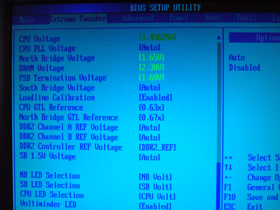
FSB Termination Voltage:
The scale runs from 1.2V-2V in .02V increments. Again, the board overvolts the BIOS setting by around 0.03V-0.04V. We recommend that users do not exceed a setting of 1.56V (1.6V actual) for 24/7 use. As FSB is raised with a quad-core CPU, VTT also needs to be raised. Expect to use between 1.5V-1.6V for overclocks past 440 FSB.
CPU GTL Reference:
Available options are, 0.57x, 0.59x, 0.61x, and 0.63x. This function controls GTL reference voltage to both CPU die's simultaneously. This is not completely ideal as there are always mismatches in CPU fabrication and motherboard components that may require individual GTL voltage level adjustments for each CPU die. The only option of use here is 0.63x, which is actually mislabeled and closer to around 66-67% of VTT. Intel specification for GTL reference voltages is 67%. We probed the on-board voltages with a DMM to find out just how close ASUS is to the 67% mark of VTT.
The closest point to 67% on our motherboard for both CPU die is 1.54V (set in BIOS). Although the differences between actual GTL and Intel 67% specification seem small, fine control of the GTL voltages would have helped the board's overall stability when pushing past 450FSB with the Quad Cores. Each board will have a different level of voltage variance due to on-board component tolerances. In short, a 0.63x setting for GTL at 1.54VTT will not equate to the same measured GTL value on every board and may be adrift from the ideal 67% specification.
NB GTL Reference:
The scale runs from 0.49x to 0.67x in 0.02X increments. 0.67% worked best on our board and processors. We found that values lower than 0.67x caused lock ups and non-boot situations. Again, finer control options would have been nice and should be expected on a board in this price range.
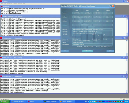
We listed our BIOS settings below for a stable 450FSB run of the Prime95 torture test (8 hours 54mins passed), for those who are interested in this type of stability. Please note that component abilities do vary from board to board; these settings are only an approximate guideline.
FSB Termination Voltage:
The scale runs from 1.2V-2V in .02V increments. Again, the board overvolts the BIOS setting by around 0.03V-0.04V. We recommend that users do not exceed a setting of 1.56V (1.6V actual) for 24/7 use. As FSB is raised with a quad-core CPU, VTT also needs to be raised. Expect to use between 1.5V-1.6V for overclocks past 440 FSB.
CPU GTL Reference:
Available options are, 0.57x, 0.59x, 0.61x, and 0.63x. This function controls GTL reference voltage to both CPU die's simultaneously. This is not completely ideal as there are always mismatches in CPU fabrication and motherboard components that may require individual GTL voltage level adjustments for each CPU die. The only option of use here is 0.63x, which is actually mislabeled and closer to around 66-67% of VTT. Intel specification for GTL reference voltages is 67%. We probed the on-board voltages with a DMM to find out just how close ASUS is to the 67% mark of VTT.
| Voltage Investigations | ||||
| BIOS Set VTT | Measured VTT | BIOS set GTL | Measured GTL | 67% of VTT |
| 1.50 | 1.53 | 0.63x | 1.022 | 1.025 |
| 1.52 | 1.55 | 0.63x | 1.036 | 1.038 |
| 1.54 | 1.57 | 0.63x | 1.051 | 1.051 |
| 1.56 | 1.60 | 0.63x | 1.065 | 1.072 |
| 1.58 | 1.62 | 0.63x | 1.080 | 1.085 |
| 1.60 | 1.64 | 0.63x | 1.090 | 1.098 |
The closest point to 67% on our motherboard for both CPU die is 1.54V (set in BIOS). Although the differences between actual GTL and Intel 67% specification seem small, fine control of the GTL voltages would have helped the board's overall stability when pushing past 450FSB with the Quad Cores. Each board will have a different level of voltage variance due to on-board component tolerances. In short, a 0.63x setting for GTL at 1.54VTT will not equate to the same measured GTL value on every board and may be adrift from the ideal 67% specification.
NB GTL Reference:
The scale runs from 0.49x to 0.67x in 0.02X increments. 0.67% worked best on our board and processors. We found that values lower than 0.67x caused lock ups and non-boot situations. Again, finer control options would have been nice and should be expected on a board in this price range.
We listed our BIOS settings below for a stable 450FSB run of the Prime95 torture test (8 hours 54mins passed), for those who are interested in this type of stability. Please note that component abilities do vary from board to board; these settings are only an approximate guideline.
| 450FSB Quad-Core BIOS Settings | |
| CPU Feature | |
| Ai Overclock Tuner | [Manual] |
| OC From CPU Level Up | [Auto] |
| CPU Ratio Control | [Manual] |
| Ratio CMOS Setting: | [8] |
| FSB Frequency | [450] |
| FSB Strap to North Bridge | [400MHz] |
| PCIE Frequency | [110] |
| DRAM Settings | |
| DRAM Frequency | [DDR2-1199MHZ] |
| DRAM Command Rate | [2T] |
| DRAM Timing Control | [Manual] |
| CAS# Latency | [5] |
| RAS# to CAS Delay | [5] |
| RAS# Precharge | [5] |
| RAS# Active Time | [12] |
| RAS# To Ras# Delay | [3] |
| Row Refresh Cycle Time | [42] |
| Write Recovery Time | [6] |
| Read To Precharge Time | [3] |
| Read To Write Delay(S/D) | [8] |
| Write To Read Delay(S) | [3] |
| Write To Read Delay(D) | [5] |
| Read To Read Delay(S) | [4] |
| Read To Read Delay(D) | [6] |
| Write To Write Delay(S) | [4] |
| Write To Write Delay(D) | [6] |
| DRAM Static Read Control | [Disabled] |
| Ai Clock Twister | [Strong] |
| Transaction Booster | [Enabled] |
| Boost Level | [0] |
| Voltage Settings | |
| CPU Voltage | [1.43125v] |
| CPU PLL Voltage | [Auto] |
| North Bridge Voltage | [1.61v] |
| DRAM Voltage | [2.16v] |
| FSB Termination Voltage | [1.54v] |
| South Bridge Voltage | [Auto] |
| Loadline Calibration | [Enabled] |
| CPU GTL Reference | [0.63x] |
| North Bridge GTL Reference | [0.67x] |
| DDR2 Channel A REF Voltage | [Auto] |
| DDR2 Channel B REF Voltage | [Auto] |
| DDR2 Controller REF Voltage | [DDR2_REF] |
| SB 1.5V Voltage | [Auto] |
| . | |
Originally published at https://www.anandtech.com/show/2374 (Wayback Machine).