
DX10 for the Masses: NVIDIA 8600 and 8500 Series Launch
- Posted in
- GPUs
Under the Hood of G84
So the quick and dirty summary of the changes is that the G84 is a reduced width G80 with a higher proportion of texture to shader hardware and a reworked PureVideo processing engine (dubbed VP2 as opposed to G80's VP1). Because there are fewer ROPs, fill rate and antialiasing capabilities will be reduced from the G80 as well. This isn't as necessary on a budget card where shader power won't be able to keep up with huge resolutions either.
We expect the target audience of the 8600 series to be running 1280x1024 resolution panels. Of course, some people will be running larger panels and we will test some higher resolutions to see what kind of capabilities the hardware has, but above 1600x1200 tests are somewhat academic. As 1080p TVs become more popular in the coming years, however, we may start putting pressure on graphics makers to target 1920x1200 as their standard resolution for mainstream parts even if average computer monitor sizes weigh in with fewer pixels.
In order to achieve playable performance at 1280x1024 with good quality settings, NVIDIA has gone with 32 shaders, 16 texture address units, and 8 ROPs. Here's the full breakdown:
We'll tackle the 8500 in more depth when we have hardware. For now, we'll include the data as reference. As for the 8600, right out of the gate, 32 SPs mean one third the clock for clock shader power of the 8800 GTS. At the same time, NVIDIA has increased the ratio of Texture address units to SPs from 1:4 to 1:2. We also see a 1:1 ratio of texture address and filter units. These changes prompted NVIDIA to further optimize their scheduling algorithms.
The combination of greater resource availability and improved scheduling allow for increased efficiency. In other words, clock for clock, G84 SPs are more efficient than G80 SPs. This makes it harder to compare performance based on specifications. Apparently stencil culling performance has also been improved, which should help boost algorithms like the Doom 3 engine's shadowing technique. NVIDIA didn't give us any detail on how stencil culling performance was improved, but indicated that this, among other things, was also tweaked with the new hardware.
Top this off with the fact that G84 has also been enhanced for higher clock speeds than G80 and we can expect much more work to be done by each SP per second than on 8800 hardware. Exactly how much is something we don't have an easy way of measuring as changes in efficiency will vary by the algorithms running on the hardware as well.
With 256 MB of memory on a 128-bit bus, we can expect a little more memory pressure than on the 8800 series. The 2 x 64-bit wide channels provide 40% of the bus width of an 8800 GTS. This isn't as cut down as the number of SPs; remember that the texture address units have only been reduced from 24 on the 8800 GTS to 16 on the 8600 series. Certainly the reduction of 20 ROPs to 8 will help cut down on memory traffic, but that extra texturing power won't be insignificant. While we don't have quantitative measurements, our impression is that memory bandwidth is more important in NVIDIA's more finely grained unified architecture than it was with the GeForce 7 series pipelined architecture. Sticking with a 128-bit memory interface for their mainstream part might work this time around, but depending on what we see from game developers over the next six months, this could easily change in the near future.
Let's round out our architectural discussion with a nice block diagram for the 8600 series:
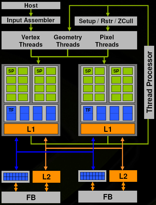
We can see very clearly that this is a cut down G80. As we have discussed, many of these blocks have been tweaked and enhanced to provide more efficient processing. The fundamental function of each block remains the same, and the inside of each SP remains unchanged as well. The features supported are also the same as G80. For 8500 hardware, based on G86, we drop down from two blocks of Shaders and ROPs to one each.
Two full dual-link DVI ports on a $150 card is a very nice addition. With the move from analog to digital displays, seeing a reduction in maximum resolution on budget parts because of single-link bandwidth limitations, while not devastating, isn't desirable. There are tradeoffs in moving from analog to digital display hardware, and now an additional issue has a resolution. Now we just need to see display makers crank up pixel density and improve color space without reducing response time and this old Sony GDM-F520 can finally rest in peace.
In the video output front, G84 makes a major improvement over all other graphics cards on the market: G84 based hardware supporting HDCP will be capable of HDCP over dual-link connections. This is a major feature, as a handful of larger widescreen monitors like Dell's 30" only support 1920x1080 with a dual-link connection. Unless both links are protected with HDCP, software players will refuse to play AACS protected HD content. NVIDIA has found a way around the problem by using one key ROM but sending the key over both links. The monitor is able to handle HDCP connections on both links, and is able to display the video properly at the right resolution.
As for manufacturing, the G84 is still an 80 nm part. While G80 is impressively huge at 681M transistors, G84 is "only" 289M transistors. This puts it at nearly the same transistor count as G71 (7900 GTX). While performance of the 8600 series doesn't quite compare to the 7900 GTX, the 80 nm process makes smaller die sizes (and lower prices) possible.
In addition to all this, PureVideo has received a significant boost this time around.
So the quick and dirty summary of the changes is that the G84 is a reduced width G80 with a higher proportion of texture to shader hardware and a reworked PureVideo processing engine (dubbed VP2 as opposed to G80's VP1). Because there are fewer ROPs, fill rate and antialiasing capabilities will be reduced from the G80 as well. This isn't as necessary on a budget card where shader power won't be able to keep up with huge resolutions either.
We expect the target audience of the 8600 series to be running 1280x1024 resolution panels. Of course, some people will be running larger panels and we will test some higher resolutions to see what kind of capabilities the hardware has, but above 1600x1200 tests are somewhat academic. As 1080p TVs become more popular in the coming years, however, we may start putting pressure on graphics makers to target 1920x1200 as their standard resolution for mainstream parts even if average computer monitor sizes weigh in with fewer pixels.
In order to achieve playable performance at 1280x1024 with good quality settings, NVIDIA has gone with 32 shaders, 16 texture address units, and 8 ROPs. Here's the full breakdown:
| GeForce 8600/8500 Hardware | |||
| GeForce 8600 GTS | GeForce 8600 GT | GeForce 8500 | |
| Stream Processors | 32 | 32 | 16 |
| Texture Address / Filtering | 16/16 | 16/16 | 8/8 |
| ROPs | 8 | 8 | 4 |
| Core Clock | 675 MHz | 540 MHz | 450 MHz |
| Shader Clock | 1.45 GHz | 1.19 GHz | 900 MHz |
| Memory Clock (Data Rate) | 2 GHz | 1.4 GHz | 800 MHz |
| Memory Bus Width | 128-bit | 128-bit | 128-bit |
| Frame Buffer | 256 MB | 256 MB | 256MB / 512MB |
| Outputs | 2x dual-link DVI | 2x dual-link DVI | ? |
| Transistor count | 289 M | 289 M | ? |
| Price | $200 - $230 | $150 - $160 | $90 - $130 |
We'll tackle the 8500 in more depth when we have hardware. For now, we'll include the data as reference. As for the 8600, right out of the gate, 32 SPs mean one third the clock for clock shader power of the 8800 GTS. At the same time, NVIDIA has increased the ratio of Texture address units to SPs from 1:4 to 1:2. We also see a 1:1 ratio of texture address and filter units. These changes prompted NVIDIA to further optimize their scheduling algorithms.
The combination of greater resource availability and improved scheduling allow for increased efficiency. In other words, clock for clock, G84 SPs are more efficient than G80 SPs. This makes it harder to compare performance based on specifications. Apparently stencil culling performance has also been improved, which should help boost algorithms like the Doom 3 engine's shadowing technique. NVIDIA didn't give us any detail on how stencil culling performance was improved, but indicated that this, among other things, was also tweaked with the new hardware.
Top this off with the fact that G84 has also been enhanced for higher clock speeds than G80 and we can expect much more work to be done by each SP per second than on 8800 hardware. Exactly how much is something we don't have an easy way of measuring as changes in efficiency will vary by the algorithms running on the hardware as well.
With 256 MB of memory on a 128-bit bus, we can expect a little more memory pressure than on the 8800 series. The 2 x 64-bit wide channels provide 40% of the bus width of an 8800 GTS. This isn't as cut down as the number of SPs; remember that the texture address units have only been reduced from 24 on the 8800 GTS to 16 on the 8600 series. Certainly the reduction of 20 ROPs to 8 will help cut down on memory traffic, but that extra texturing power won't be insignificant. While we don't have quantitative measurements, our impression is that memory bandwidth is more important in NVIDIA's more finely grained unified architecture than it was with the GeForce 7 series pipelined architecture. Sticking with a 128-bit memory interface for their mainstream part might work this time around, but depending on what we see from game developers over the next six months, this could easily change in the near future.
Let's round out our architectural discussion with a nice block diagram for the 8600 series:
We can see very clearly that this is a cut down G80. As we have discussed, many of these blocks have been tweaked and enhanced to provide more efficient processing. The fundamental function of each block remains the same, and the inside of each SP remains unchanged as well. The features supported are also the same as G80. For 8500 hardware, based on G86, we drop down from two blocks of Shaders and ROPs to one each.
Two full dual-link DVI ports on a $150 card is a very nice addition. With the move from analog to digital displays, seeing a reduction in maximum resolution on budget parts because of single-link bandwidth limitations, while not devastating, isn't desirable. There are tradeoffs in moving from analog to digital display hardware, and now an additional issue has a resolution. Now we just need to see display makers crank up pixel density and improve color space without reducing response time and this old Sony GDM-F520 can finally rest in peace.
In the video output front, G84 makes a major improvement over all other graphics cards on the market: G84 based hardware supporting HDCP will be capable of HDCP over dual-link connections. This is a major feature, as a handful of larger widescreen monitors like Dell's 30" only support 1920x1080 with a dual-link connection. Unless both links are protected with HDCP, software players will refuse to play AACS protected HD content. NVIDIA has found a way around the problem by using one key ROM but sending the key over both links. The monitor is able to handle HDCP connections on both links, and is able to display the video properly at the right resolution.
As for manufacturing, the G84 is still an 80 nm part. While G80 is impressively huge at 681M transistors, G84 is "only" 289M transistors. This puts it at nearly the same transistor count as G71 (7900 GTX). While performance of the 8600 series doesn't quite compare to the 7900 GTX, the 80 nm process makes smaller die sizes (and lower prices) possible.
In addition to all this, PureVideo has received a significant boost this time around.
Originally published at https://www.anandtech.com/show/2213 (Wayback Machine).