
EVGA nForce 650i Ultra: Performance on a Budget
- Posted in
- Motherboards
NVIDIA nForce 650i Ultra Chipset Features
Before we get to our initial performance results and discussion of this budget 650i Ultra board design we need to first explain the differences between it and the other Intel chipset offerings from NVIDIA.
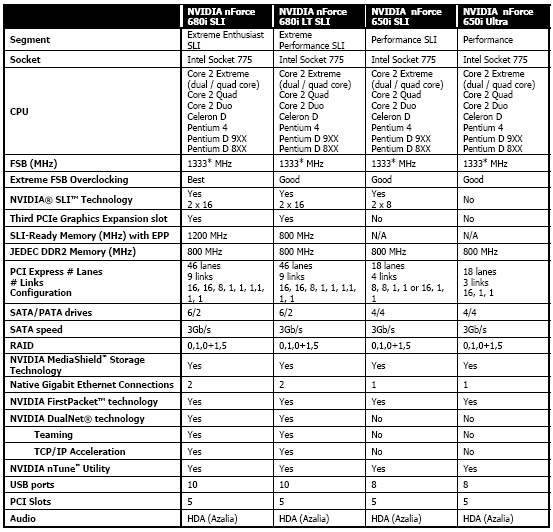
All of the chipsets offer support for the latest Intel Socket 775 based processors along with official 1333FSB speeds for the upcoming 1333FSB based CPUs. The 650i SLI and 650i Ultra chipsets are based on the same 650i SPP and utilize the nF430 MCP. The only differentiator between the two is how this SPP/MCP combination is implemented on a board with the 650i SLI offering SLI operation at 8x8 compared to the single x16 slot on the 650i Ultra.
Other differences between the chipsets center on the features that the 680i offers that are not available on the 650i. These features include two additional USB 2.0 ports, two additional SATA ports, an additional Gigabit Ethernet port, Dual-Net technology, and EPP memory support. Otherwise, depending upon BIOS tuning, the performance of the chipsets is very similar across a wide range of applications, with overclocking capabilities being slightly more pronounced on the 680i chipset. In our testing we have found that the other chipsets also offer very good overclocking capabilities with SLI performance basically being equal at common resolutions on supported chipsets.
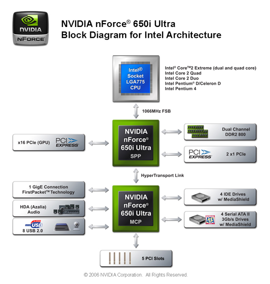
This diagram lists the basic features of the 650i Ultra chipset. The differences between the available options and our EVGA 650i Ultra board is the removal of an IDE port that would support two additional PATA drives and two less PCI slots. The inclusion of the additional IDE port could have benefited this board considering the price range, particularly for those interested in using older IDE hard drives to keep upgrade costs down.
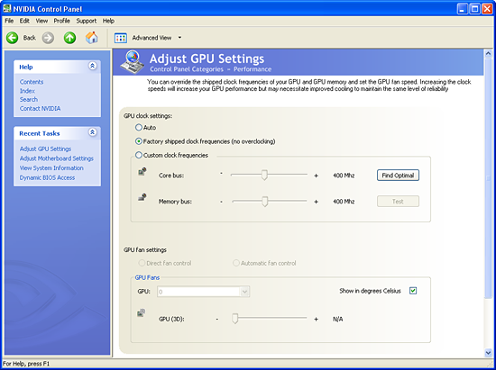
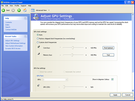
One of the new features being implemented by NVIDIA with the 650i Ultra release is an automatic GPU optimization capability. These optimizations are handled automatically by the GPU and board driver sets based upon the installed GPU and BIOS support. Initial support is for the 7600GS and 7300GT video cards but it will be expanded across a wider range of NVIDIA based graphic cards in the near future. We will also see more aggressive tuning as this technology matures over time.
The drivers will determine a safe overclocking level for the GPU and then implement the changes automatically. This support is transparent to the user and works seamlessly. We tested this feature exhaustively across a wide range of applications and it never once created an issue. These optimizations provided a 2% to 4% improvement in our game benchmark scores.
Obviously, the more astute computer user can get the same or better results by manually overclocking the GPU which is why some users will probably think of this as a gimmick. However, we believe any time you can gain performance at no cost or effort then there's not reason to complain.
Before we get to our initial performance results and discussion of this budget 650i Ultra board design we need to first explain the differences between it and the other Intel chipset offerings from NVIDIA.
All of the chipsets offer support for the latest Intel Socket 775 based processors along with official 1333FSB speeds for the upcoming 1333FSB based CPUs. The 650i SLI and 650i Ultra chipsets are based on the same 650i SPP and utilize the nF430 MCP. The only differentiator between the two is how this SPP/MCP combination is implemented on a board with the 650i SLI offering SLI operation at 8x8 compared to the single x16 slot on the 650i Ultra.
Other differences between the chipsets center on the features that the 680i offers that are not available on the 650i. These features include two additional USB 2.0 ports, two additional SATA ports, an additional Gigabit Ethernet port, Dual-Net technology, and EPP memory support. Otherwise, depending upon BIOS tuning, the performance of the chipsets is very similar across a wide range of applications, with overclocking capabilities being slightly more pronounced on the 680i chipset. In our testing we have found that the other chipsets also offer very good overclocking capabilities with SLI performance basically being equal at common resolutions on supported chipsets.
This diagram lists the basic features of the 650i Ultra chipset. The differences between the available options and our EVGA 650i Ultra board is the removal of an IDE port that would support two additional PATA drives and two less PCI slots. The inclusion of the additional IDE port could have benefited this board considering the price range, particularly for those interested in using older IDE hard drives to keep upgrade costs down.
One of the new features being implemented by NVIDIA with the 650i Ultra release is an automatic GPU optimization capability. These optimizations are handled automatically by the GPU and board driver sets based upon the installed GPU and BIOS support. Initial support is for the 7600GS and 7300GT video cards but it will be expanded across a wider range of NVIDIA based graphic cards in the near future. We will also see more aggressive tuning as this technology matures over time.
The drivers will determine a safe overclocking level for the GPU and then implement the changes automatically. This support is transparent to the user and works seamlessly. We tested this feature exhaustively across a wide range of applications and it never once created an issue. These optimizations provided a 2% to 4% improvement in our game benchmark scores.
Obviously, the more astute computer user can get the same or better results by manually overclocking the GPU which is why some users will probably think of this as a gimmick. However, we believe any time you can gain performance at no cost or effort then there's not reason to complain.
Originally published at https://www.anandtech.com/show/2207 (Wayback Machine).