
EVGA 680i LT SLI: NVIDIA's 680i Cost Reduced
- Posted in
- CPUs
Features and Specifications
The NVIDIA reference BIOS offers a moderate level of options available for tweaking the board with emphasis placed on the available memory settings. We found in memory testing that switching to manual settings and changing the tCAS, tRCD, tRP, and tRAS was required to ensure optimum performance as our performance results will show shortly.
Compared to the standard 680i BIOS the ability to control the HT and MCP voltages is not available, and FSB and SPP voltages are limited to 1.4V. The inability to change FSB VTT or GTL Ref voltage settings limited our overclocking results to some degree, but more importantly the lack of higher FSB/SPP voltages basically capped our board sample at 500FSB.
One other issue we have with the "Lite" BIOS is that memory voltages are limited to .10V increments meaning that in several cases we could not fine tune our ProMOS or Elpida modules for optimum performance. While we understand NVIDIA's desire not to have this board compete directly with the 680i boards, some of the cuts made are generally frustrating for extracting the best performance out of this board.
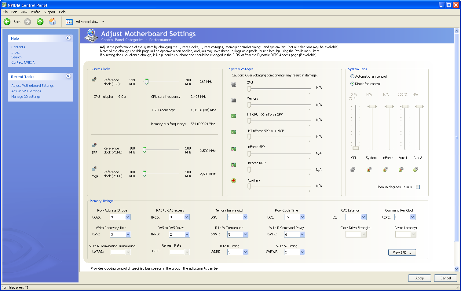
EVGA utilizes the standard NVIDIA nTune system utility but in yet another weird BIOS decision the ability to control voltages and fan speeds is non-existent. This ensures that any significant changes required for overclocking the board will have to be done via the BIOS. This is an operation that most people normally do anyway when overclocking, but one of the strengths of NVIDIA's reference boards has been their tight integration with nTune. The inability to control even the CPU fan is inexcusable considering this is a designed by NVIDIA board. Hopefully, the next BIOS release will address these two issues, and we certainly would like see additional voltage controls and automatic fan speed control for the other chassis fan headers. Of course, NVIDIA could really surprise us and offer fan control over the active chipset coolers.
| EVGA 680i LT SLI | |
| Market Segment: | High-End Performance - $199 |
| CPU Interface: | Socket T (Socket 775) |
| CPU Support: | LGA775-based Pentium 4, Celeron D, Pentium D, Pentium EE, Core 2 Duo, Core 2 Extreme |
| Chipset: | NVIDIA 680i LT SPP (C55 P-N-A2) + 680i LT MCP (570 SLI MCP) |
| Bus Speeds: | Auto, 400 to 2500 QDR (100~625) in 1MHz increments |
| Memory Ratios: | Auto, Sync., 1:1, 5:4, 3:2 |
| Memory Speed: | 400MHz~1400MHz in various increments |
| PCIe 1&2 Speeds: | 100MHz~200MHz in 1MHz Increments |
| HT Multipliers: | 1x, 2x, 3x, 4x, 5x |
| Core Voltage: | Auto, 0.80000V to 1.60000 in 0.00625V increments |
| FSB Options: | Auto, Linked, Unlinked |
| CPU Clock Multiplier: | Auto, 6x-11x in 1X increments - Core 2 Duo, downwards unlocked, Core 2 Extreme 6x-60X |
| DRAM Voltage: | Auto, 1.80V to 2.50 in .10V increments |
| DRAM Timing Control: | Optimal, Expert - 10 DRAM Timing Options |
| NB Voltage: | Auto, 1.2V, 1.3V, 1.4V |
| FSB Voltage: | Auto, 1.2V, 1.3V, 1.4V |
| Memory Slots: | Four 240-pin DDR2 DIMM Slots Dual-Channel Configuration, DDR2-400, 533, 667, 800 Regular Unbuffered Memory to 8GB Total |
| Expansion Slots: | 2 - PCIe X16 (2-x16 electrical for SLI or Multi-GPU) 2 - PCIe x1 2 - PCI Slot 2.2 |
| Onboard SATA/RAID: | 6 SATA 3Gbps Ports - 570 SLI MCP (RAID 0,1, 0+1, 5, JBOD) |
| Onboard IDE: | 1 ATA133/100/66 Port (2 drives) - 570 SLI MCP |
| Onboard USB 2.0/IEEE-1394: | 8 USB 2.0 Ports - 4 I/O Panel - 4 via Headers 2 Firewire 400 Ports by TI TSB43AB22A - 1 I/O Panel, 1 via Header |
| Onboard LAN: | NVIDIA Gigabit Ethernet - PCIe - Marvell 88E1116 PHY - 1 port via 570 SLI MCP |
| Onboard Audio: | Realtek ALC885 - 8-channel HD audio codec |
| Power Connectors: | ATX 24-pin, 8-pin EATX 12V, 4-pin 12V Molex |
| I/O Panel: | 1 x PS/2 Keyboard 1 x PS/2 Mouse 1 x S/PDIF Optical - Out 1 x IEEE 1394a 1 x Audio Panel 1 x RJ45 4 x USB 2.0/1.1 |
| BIOS Revision: | Award 721N0P01 |
| Board Revision: | v1.0 |
The NVIDIA reference BIOS offers a moderate level of options available for tweaking the board with emphasis placed on the available memory settings. We found in memory testing that switching to manual settings and changing the tCAS, tRCD, tRP, and tRAS was required to ensure optimum performance as our performance results will show shortly.
Compared to the standard 680i BIOS the ability to control the HT and MCP voltages is not available, and FSB and SPP voltages are limited to 1.4V. The inability to change FSB VTT or GTL Ref voltage settings limited our overclocking results to some degree, but more importantly the lack of higher FSB/SPP voltages basically capped our board sample at 500FSB.
One other issue we have with the "Lite" BIOS is that memory voltages are limited to .10V increments meaning that in several cases we could not fine tune our ProMOS or Elpida modules for optimum performance. While we understand NVIDIA's desire not to have this board compete directly with the 680i boards, some of the cuts made are generally frustrating for extracting the best performance out of this board.
 |
| Click to enlarge |
EVGA utilizes the standard NVIDIA nTune system utility but in yet another weird BIOS decision the ability to control voltages and fan speeds is non-existent. This ensures that any significant changes required for overclocking the board will have to be done via the BIOS. This is an operation that most people normally do anyway when overclocking, but one of the strengths of NVIDIA's reference boards has been their tight integration with nTune. The inability to control even the CPU fan is inexcusable considering this is a designed by NVIDIA board. Hopefully, the next BIOS release will address these two issues, and we certainly would like see additional voltage controls and automatic fan speed control for the other chassis fan headers. Of course, NVIDIA could really surprise us and offer fan control over the active chipset coolers.
Originally published at https://www.anandtech.com/show/2198 (Wayback Machine).