
The Era of Tera: Intel Reveals more about 80-core CPU
- Posted in
- CPUs
The Architecture
Despite being built on a large die, the individual tiles in the Teraflops chip are extremely simple cores. These aren't x86 cores, although Intel indicated that one of the next steps for the project was to integrate x86 cores. At a high level, each tile is composed of a Processing Engine (PE) to handle all computations and a 5-port router to pass data from one tile to the next.
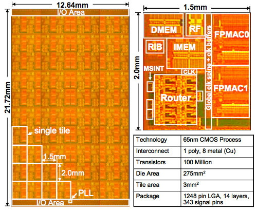
In order to keep the tile hardware as simple as possible, the tiles are based on a 96-bit Very Long Instruction Word (VLIW) architecture. Intel's other famous VLIW architecture is of course the Itanium, but there's very little else that's in common between the two designs. In short, a VLIW architecture simplifies hardware design by relying on the compiler to schedule instructions for execution rather than having the CPU figure out how to dynamically parallelize and schedule operations. VLIW isn't common for desktop architectures, but for specialized applications it's not far fetched. The number of applications you've got to run on these things is limited, and thus adding complexity on the compiler side isn't such a bad tradeoff.
There are obvious drawbacks to going with a VLIW architecture, but it appears that Intel's fundamental goals with the teraflops chip were to deal with implementing a many-core CPU and not necessarily deliver a high performance one.
The processing engine is composed of a 3KB single-cycle instruction memory, 2KB data memory, 10-port register file, and two single-cycle throughput single-precision floating point multiply-accumulator units.
A maximum of 8 operations can be encoded in a single VLIW instruction on the teraflops chip. Those operations can be FPMACs, loads/stores, as well as instructions to the router on each tile as each tile can pass data and instructions on to any adjacent tile.
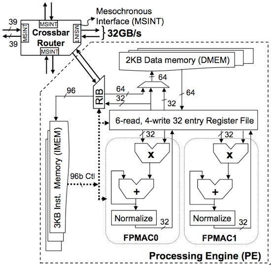
Although the chip itself is capable of processing over one trillion floating point operations per second, don't be fooled by the numbers; these aren't 128-bit FP operations but rather single-precision FP operations. Each tile features two fully pipelined 32-bit floating point multiple-accumulator (FPMAC) units. There are no other execution units on each tile, so all arithmetic operations must be carried out through these FPMACs. This obviously limits the applications that the teraflops chip can be used in, but it also supports the idea that the point of this chip isn't to break speed barriers, but rather develop a framework to introduce other more capable processors with many cores. The real focus here isn't on the floating point throughput of the array of tiles; instead, the primary objective is to work on the network that connects the tiles together.
Originally published at https://www.anandtech.com/show/2170 (Wayback Machine).