
AMD Launches Carrizo: The Laptop Leap of Efficiency and Architecture Updates
Efficiency and Die Area Savings
AMD’s take home message in all of this is efficiency. We a being quoted a performance per watt increase of 2.4x, coming from typical power draw savings of 2x and performance increase of almost 1.5x for 23% less die area, all in one go.
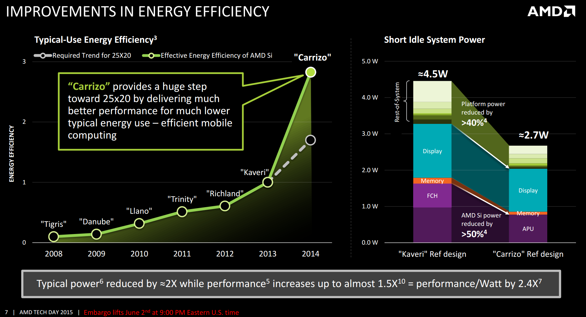
Ultimately this all helps AMD’s plan to be 25x more efficient with their APUs by 2020, and the cumulative bar chart on the right is how mobile improvements from all sides are being realized. Migrating the southbridge on die severely reduces its idle power consumption to almost zero and can help efficiencies elsewhere in the system. The APU general use and memory controllers are the next targets, but the common constant here is the display. Using a low power display might give battery life in exchange for quality, and there is only so much power you can save at the SoC level. In time, the display will be the main focus of power saving for these devices.
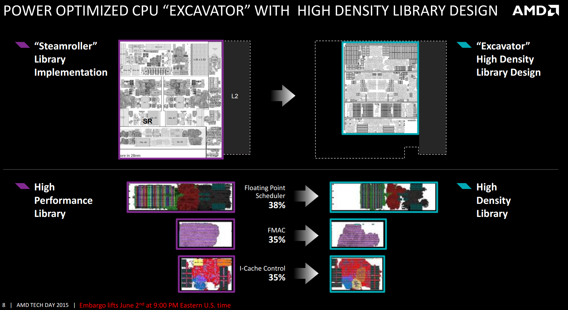
A big part of the reduction in die area comes from the set of high density libraries being used by AMD. Above were three examples provided where >33% gains were made in silicon area. Typically using a high density library design is a double edged sword – it reduces die area and potentially leaves more area for other things, but the caveat is that it may be more prone to defects in construction, require additional latency or have a different frequency/voltage profile. AMD assures us that these changes are at least like-for-like but most of them contain other improvements as well.
It’s worth noting here that AMD has described the high density library project internally as the equivalent of a moonshot, essentially the developers were part of a ‘skunkworks’ division attempting to make drastic changes in order to improve performance. The high density library is one such successful project from that.
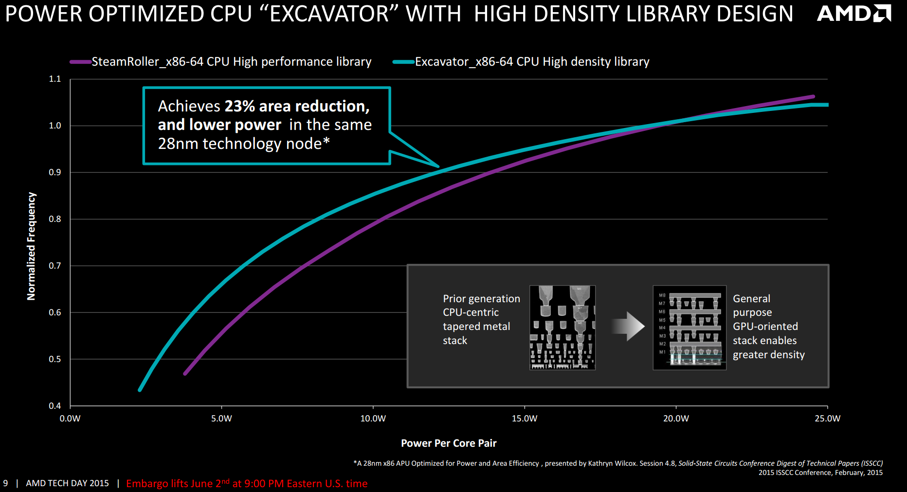
With the new libraries, comparing Excavator to Steamroller shows the effect moving designs has. The power/frequency curve below 20W per module shifts to higher frequency/lower power, whereas losses are observed above 20W. However for 15W per module, this means either a 10%+ power reduction at the same frequency or a 5% increase in frequency for the same power. Should AMD release dual thread / single core APUs in the 7.5W region, this is where most of the gains are (as noted in the comments, the dual module designs are at 7.5W per module, meaning that what we should see in devices is already in the peak value for gains and benefits such as 25% frequency or 33% power). As also seen in the insert, the silicon stack has been adjusted to a more general purpose orientation. I could comment that this makes the CPU and GPU work better together, but I have no way of verifying this. AMD states the change in the silicon stack makes production slightly easier but also helps with achieving the higher density Excavator exhibits.
Originally published at https://www.anandtech.com/show/9319/amd-launches-carrizo-the-laptop-leap-of-efficiency-and-architecture-updates (Wayback Machine).