
The Battle of Bay Trail-D: GIGABYTE J1900N-D3V and ASUS J1900I-C Reviewed
ASUS J1900I-C Visual Inspection
The implementation of J1900 from ASUS differs a fair amount from GIGABYTE. Taking the board out of the box and the first thing to notice is the DRAM placement – instead of stacking one above the other, the modules are arranged such that one is above the SoC and one is to the right. There is still enough space for standard sized modules in both of these slots, and ASUS has even placed a fair amount of electronics underneath as well – the top DRAM slot has the Nuvoton SuperIO IC in that area, for example.
Similar to GIGABYTE, the motherboard has only two fan headers. The CPU header is below the socket beside the CR2032 battery, with the CHA header just to the left of the DRAM slot at the top. Both of these headers are 4-pin as well.
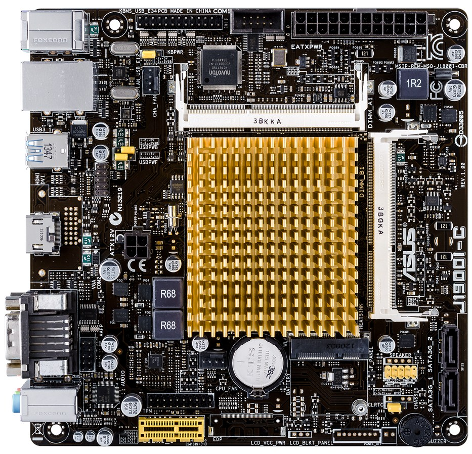
ASUS has prioritized different connectors around the edge, with the LPT header and COM header having priority at the top over the 4-pin CPU power connector which has a spot just to the left of middle nearer the SoC. This is an abysmal place for a 4-pin CPU power connector as it means any cable has to stretch over most of the board in order to reach. While making a neat layout might not be the ultimate goal for anyone using a Bay Trail motherboard, having this connector here might still disrupt airflow over the passive heatsink.
On the right hand side of the motherboard are our two SATA ports with the front panel header in yellow beside them and the internal buzzer nearby. The mini-PCIe port also rests in this bottom right corner beside the battery. Another difference to the GIGABYTE board will be the extra slot at the bottom – where GIGABYTE used a PCIe to PCI bridge, ASUS has implemented a PCIe 2.0 x1 slot instead. Perhaps unfortunately this is a closed ended PCIe 2.0 x1 slot, meaning that larger cards cannot be used. Above this is a TPM header.
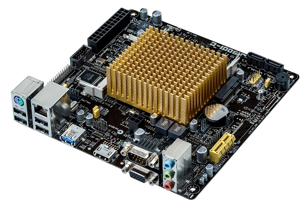
Also on the board is the front audio header, powered from a Realtek ALC887-VC audio codec, and a USB 2.0 header behind the USB 3.0 on the rear panel.
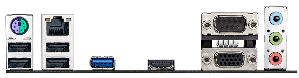
The rear panel looks a bit bleak compared to the GIGABYTE, but this is because ASUS has decided to only use one COM header here and we get HDMI rather than a DVI-D. There is also only one network port, and the PS/2 connector is a joint connector. Where GIGABYTE uses a USB 3.0 hub to have four USB 3.0 ports, the J1900I-C only has one and four USB 2.0 ports instead.
Board Features
| ASUS J1900I-C | |
| Price | Link |
| Size | Mini-ITX |
| CPU Interface | Soldered |
| Chipset | Bay Trail-D Quad Core |
| Memory Slots | Two DDR3L SO-DIMM slots supporting up to 8GB Up to Dual Channel, 1333 MHz |
| Video Outputs | VGA (2560x1600 at 60Hz) HDMI (1920x1080 at 60 Hz) |
| Onboard LAN | Realtek 8111G |
| Onboard Audio | Realtek ALC887 |
| Expansion Slots | 1 x PCIe 2.0 x1 1 x Mini-PCIe |
| Onboard SATA/RAID | 2 x SATA 3 Gbps |
| USB 3.0 | 1 x USB 3.0 (SoC) [rear panel] |
| Onboard | 2 x SATA 1 x USB 2.0 Header 1 x LPT Header 1 x COM Header 1 x TPM Header 1 x mini-PCIe 2 x Fan Headers Front Panel Header Front Audio Header |
| Power Connectors | 1 x 24-pin ATX 1 x 4-pin CPU |
| Fan Headers | 1 x CPU (4-pin) 1 x CHA (4-pin) |
| IO Panel | 1 x PS/2 Combination Port 4 x USB 2.0 Ports 1 x USB 3.0 Ports 1 x Realtek Network Port HDMI VGA 1 x COM Port Audio Jacks |
| Product Page | Link |
One might ask why the J1900N-D3V costs less than the J1900I-C and yet has two NICs and four USB 3.0 ports. The J1900I-C combats this with a HDMI port (which will arguably be preferred), have a total of six USB 2.0 ports and a PCIe 2.0 x1 port, which should also be more versatile.
Originally published at https://www.anandtech.com/show/8595/the-battle-of-bay-trail-d-gigabyte-j1900n-d3v-asus-j1900i-c-review (Wayback Machine).