
NVIDIA nForce Computex 2001 Preview
- Posted in
- CPUs
The Basics
The nForce chipset is made up of two parts, a north and south bridge, just like any other chipset. In accordance with NVIDIA's trend towards naming things as "processors," the north bridge is known as an Integrated Graphics Processor (IGP) while the south bridge gets the distinction of Media and Communications Processor (MCP).
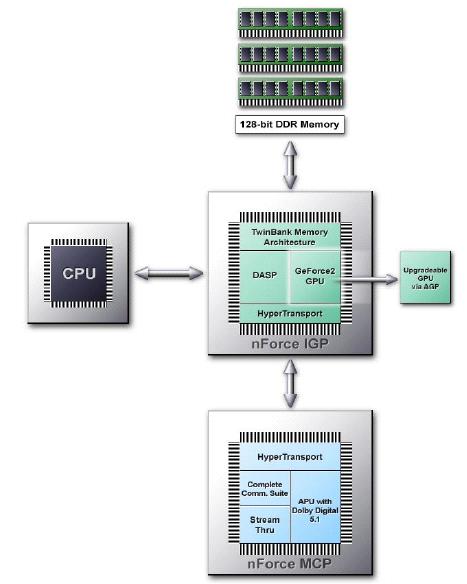
AMD's Hyper-Transport is used to link the two chips with much more bandwidth than any traditional chipset out there right now or on the horizon. At the same time, TwinBank memory architecture provides a 128-bit, 133 MHz DDR memory interface for a total of 4.2GB/s of memory bandwidth, also more than any traditional chipset.
Let's take a look at these individual components in depth to get an idea of what the nForce is really capable of.
Originally published at https://www.anandtech.com/show/781 (Wayback Machine).