
Chipset Guide
- Posted in
- Guides
 |
With the success of the original Apollo VP chipset, a supposed competitor of the Intel 430FX chipset although it blew it away in most instances, VIA decided to implement some next generation features into their hot topic VPX chipset. By raising the cacheable memory limit to 512MB, giving the user a maximum of 2MB of L2 cache, and allowing us to take advantage of such features as UltraDMA hard drives and SDRAM (features only found in Intel's TX and LX chipsets) VIA accomplished in producing a superior product in nearly every aspect to Intel's lackluster 430 series of chipsets. VIA embraced all CPU manufacturers with the release of the Apollo VPX by allowing support for normal Intel Burst Modes as well as the elusive Linear Burst Mode reserved for IBM/Cyrix processors. |
Unfortunately many motherboard manufacturers couldn't properly harness this power, and therefore quite a few users were disappointed with VPX based systems since they were poorly designed. However, a few companies were able to take advantage of the amazing capabilities of this chipset. Among these companies, FIC, seemed to be the most successful in achieving the maximum potential of the VPX chipset with their PA-2010+.
The VPX chipset features many of the useful options we all loved from the HX and VX chipsets, while adding some of its own unique characteristics such as BEDO DRAM support with a timing of 5-1-1-1. The VPX, like Intel's VX chipset supports UMA and SDRAM, however the VPX's SDRAM timings are much faster than those of Intel's VX chipset. If you combine the extensive memory support of the VPX chipset, as well as its support for UltraDMA/33 hard drives the VPX begins to look much less like a competitor and much more like a dominator in the chipset industry.
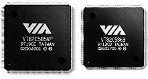
| The VPX chipset is also fully PC97 compliant, however a more affordable version without PC97 compliance is available for entry level systems consisting of the VT82C585VPX and VT82C586A instead of the VT82C585VPX north bridge and VT82C586B south bridge controllers. |  |
| VIA VT82C580VPX Apollo VPX/97 Chipset | ||
| Common Name | Apollo VPX/97 | |
| Chipset Packaging | Number of chips | 2 (VT82C595 North Bridge Controller, VT82C586B South Bridge) |
| Packaging Type | 2 x 208-pin QFP | |
| CPU Support | Number of CPUs | 1 |
| AMD CPUs Supported | K5, K6 | |
| Cyrix CPUs Supported | 6x86 (M1), 6x86MX (M2) w/ Linear Burst Mode | |
| Intel CPUs Supported | Pentium, Pentium MMX | |
| Cache | Type | Asynchronous/Synchronous Pipeline Burst Cache |
| Maximum Supported Size | 2048KB | |
| Maximum Cacheable DRAM Area | 512MB | |
| Memory | Maximum DRAM Supported | 512MB |
| BEDO DRAM Read Timings (66MHz) | 5-1-1-1 | |
| EDO DRAM Read Timings (66MHz) | 5-2-2-2 | |
| FPM DRAM Read Timings (66MHz) | 5-3-3-3 | |
| SDRAM Read Timings (66MHz) | 3-1-1-1 | |
| Data Path to Memory | 64-bits | |
| ECC Support | No | |
| Hard Disk Controller | Chip | VIA South Bridge Controller (VT82C586B) |
| Busmastering Support | Yes | |
| UltraDMA Support | Yes | |
| Max. Theoretical Transfer Rate | PIO Mode 5/DMA Mode 3 (33.3MB/S) | |
| PCI Interface | Supported PCI Bus Speeds | 25, 30, 33 MHz |
| Concurrent PCI | Yes | |
| Async. PCI Bus Speed | Yes | |
| PCI Specification | 2.0 (66 MHz max.) | |
| Power Management | PC97 Compliance | Yes |
| Suspend to Disk | Yes | |
| HDD Power Down | Yes | |
| Modem Wakeup | Yes | |
| System Suspend | Yes | |
| Video | AGP Support | No |
| Unified Memory Architecture | Yes | |
| Peripheral Support | USB Support | Yes |
| Plug and Play Port | Yes | |
| Write Buffers | CPU-to-DRAM | 16 QWords |
| CPU-to-PCI | 6 DWords | |
| PCI-to-DRAM | 48 DWords | |
| Officially Supported Bus Speeds | 50, 60, 66, 75 MHz | |
| Unofficially Achieved Bus Speeds | 68, 83.3 MHz | |
Originally published at https://www.anandtech.com/show/72 (Wayback Machine).