
Intel's Ivy Bridge Architecture Exposed
Cache, Memory Controller & Overclocking Changes
Despite the title of this section, to my knowledge there haven't been any changes to Ivy Bridge's cache. The last level cache (L3) is still shared via a ring bus between all cores, the GPU and the system agent. Quad-core Ivy Bridge CPUs will support up to 8MB of L3 cache, and the private L1/L2s haven't increased from their sizes in Sandy Bridge (32+32K/256K).
The memory controller also remains relatively unchanged, aside from some additional flexibility. Mobile IVB supports DDR3L in addition to DDR3, enabling 1.35V memory instead of the standard 1.5V DDR3. This is particularly useful in notebooks that have on-board DDR3 on the underside of the notebook; OEMs can use DDR3L and keep your lap a bit cooler.
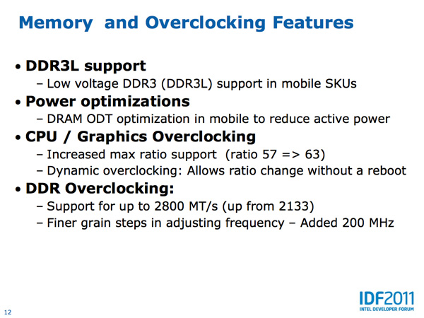
From Nehalem to Sandy Bridge, Intel introduced fairly healthy amounts of power gating throughout the processor. With little more to address in Ivy Bridge, Intel power gated one of the last available portions of the die: the DDR3 interface. If there's no external memory activity, the DDR3 interface can now be turned off completely. External IOs leak current like any other transistor so this change makes sense. Power gating simply increases die size but at 22nm Intel should have some extra area to spend on things like this.
Memory overclocking also gets a bump in Ivy Bridge. The max supported DDR3 frequency in SNB was 2133MHz, Ivy Bridge moves this up to 2800MHz. You can now also increase memory frequency in 200MHz increments.
Originally published at https://www.anandtech.com/show/4830/intels-ivy-bridge-architecture-exposed (Wayback Machine).