
The AMD Llano Notebook Review: Competing in the Mobile Market
The Llano A-Series APU
Although Llano is targeted solely at the mainstream, it is home to a number of firsts for AMD. This is AMD's first chip built on a 32nm SOI process at GlobalFoundries, it is AMD's first microprocessor to feature more than a billion transistors, and as you'll soon see it's the first platform with integrated graphics that's actually worth a damn.
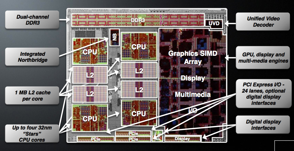
AMD is building two distinct versions of Llano, although only one will be available at launch. There's the quad-core, or big Llano, with four 32nm CPU cores and a 400 core GPU. This chip weighs in at 1.45 billion transistors, nearly 50% more than Sandy Bridge. Around half of the chip is dedicated to the GPU however, so those are tightly packed transistors resulting in a die size that's only 5% larger than Sandy Bridge.
| CPU Specification Comparison | ||||||||
| CPU | Manufacturing Process | Cores | Transistor Count | Die Size | ||||
| AMD Llano 4C | 32nm | 4 | 1.45B | 228mm2 | ||||
| AMD Llano 2C | 32nm | 2 | 758M | ? | ||||
| AMD Thuban 6C | 45nm | 6 | 904M | 346mm2 | ||||
| AMD Deneb 4C | 45nm | 4 | 758M | 258mm2 | ||||
| Intel Gulftown 6C | 32nm | 6 | 1.17B | 240mm2 | ||||
| Intel Nehalem/Bloomfield 4C | 45nm | 4 | 731M | 263mm2 | ||||
| Intel Sandy Bridge 4C | 32nm | 4 | 995M | 216mm2 | ||||
| Intel Lynnfield 4C | 45nm | 4 | 774M | 296mm2 | ||||
| Intel Clarkdale 2C | 32nm | 2 | 384M | 81mm2 | ||||
| Intel Sandy Bridge 2C (GT1) | 32nm | 2 | 504M | 131mm2 | ||||
| Intel Sandy Bridge 2C (GT2) | 32nm | 2 | 624M | 149mm2 | ||||
Given the transistor count, big Llano has a deceptively small amount of cache for the CPU cores. There is no large catch-all L3 and definitely no shared SRAM between the CPU and GPU, just a 1MB private L2 cache per core. That's more L2 cache than either the 45nm quad-core Athlon II or Phenom II parts.
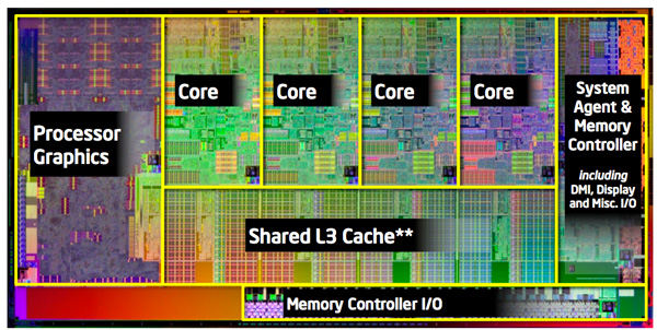
Intel's Sandy Bridge die is only ~20% GPU
The little Llano is a 758 million transistor dual-core version with only 240 GPU cores. Cache sizes are unchanged; little Llano is just a smaller version for lower price points. Initially both quad- and dual-core parts will be serviced by the same 1.45B transistor die. Defective chips will have unused cores fused off and will be sold as dual-core parts. This isn't anything unusual, AMD, Intel and NVIDIA all use die harvesting as part of their overall silicon strategy. The key here is that in the coming months AMD will eventually introduce a dedicated little Llano die to avoid wasting fully functional big Llano parts on the dual-core market. This distinction is important as it indicates that AMD isn't relying on die harvesting in the long run but rather has a targeted strategy for separate market segments.
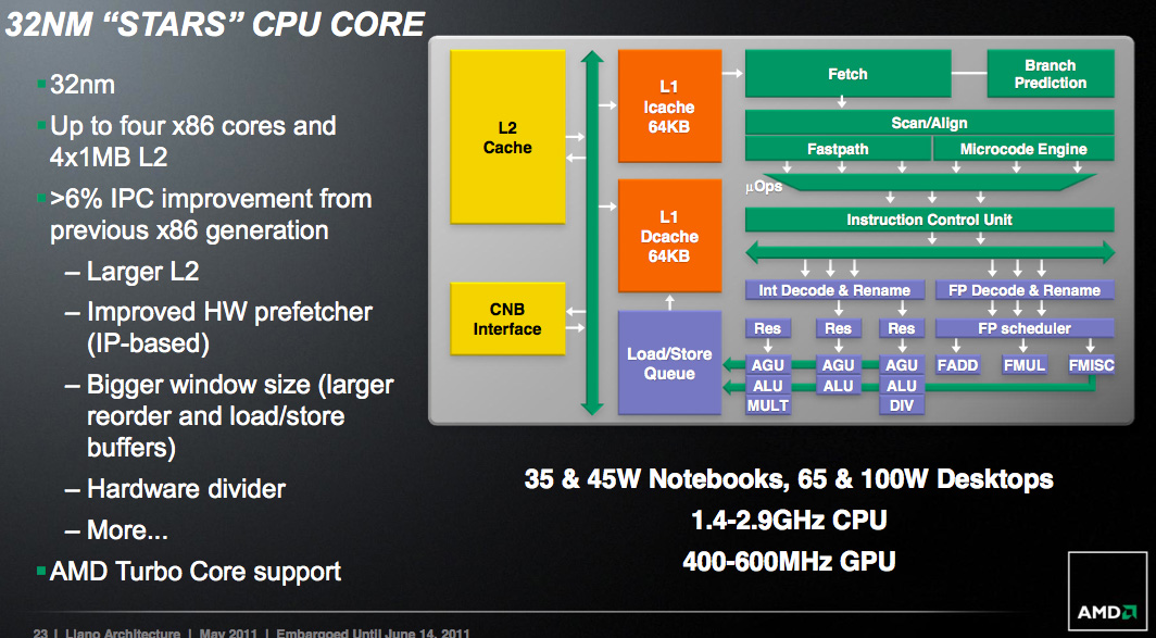
Architecturally AMD has made some minor updates to each Llano core. AMD is promising more than a 6% increase in instructions executed per clock (IPC) for the Llano cores vs. their 45nm Athlon II/Phenom II predecessors. The increase in IPC is due to the larger L2 cache, larger reorder and load/store buffers, new divide hardware, and improved hardware prefetchers.
On average I measured around a 3% performance improvement at the same clock speed as AMD's 45nm parts. Peak performance improved up to 14% however most of the gains were down in the 3—5% range. This is arguably the biggest problem that faces Llano. AMD's Phenom architecture debuted in 2007 and was updated in 2009. Llanos cores have been sitting around for the past 3-4 years with only a mild update while Intel has been through two tocks in the same timeframe. A ~6% increase in IPC isn't anywhere near close enough to bridge the gap left by Nehalem and Sandy Bridge.
Note that this comparison is without AMD's Turbo Core enabled, but more on that later.
Originally published at https://www.anandtech.com/show/4444/amd-llano-notebook-review-a-series-fusion-apu-a8-3500m (Wayback Machine).