
ASUS M4A89GTD Pro - A Core Unlocking 890GX for $140
- Posted in
- Motherboards
Board Layout
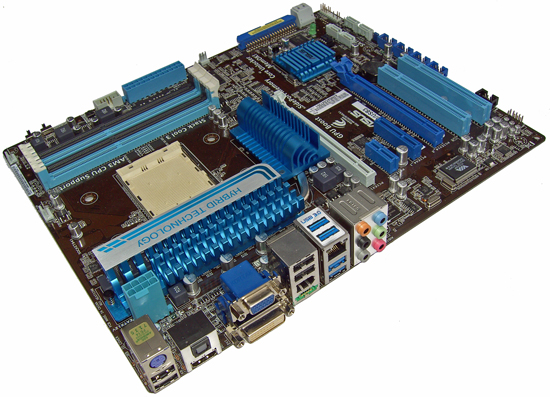
Board layout is good, with most slots and connectors placed for easy access. It looks like ASUS have not skimped on the CPU VRM for this board as it's rated for 180 amps, which is good news with Thuban on the horizon.
The IGP and CPU FET heatsinks are connected via a heatpipe, which provides the GPU a little extra mass to dissipate heat. The CPU FET portion of the heatsink is attached to the board with push-pins; it’s a long assembly so a back plate with screw fittings would ensure better contact for the central FETs when the PCB bows from the pressure of some CPU coolers. Operating temperatures are good though, needing little cross-flow when overclocking to keep things cool.
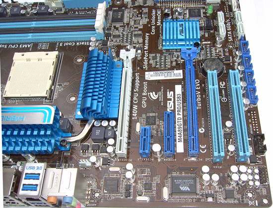
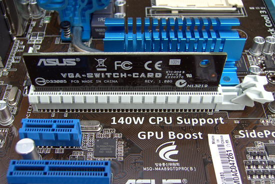
There’s always a design oddity somewhere on a motherboard and the picture above is the M4A89GTD Pro’s unsightly wart. ASUS have not used PCIe lane switches on this board, which means you have to insert that little PCB to enjoy 16x bandwidth to the central PEG slot. The top (white) PEG slot runs on an 8x lane allocation at all times, regardless of slot loading.
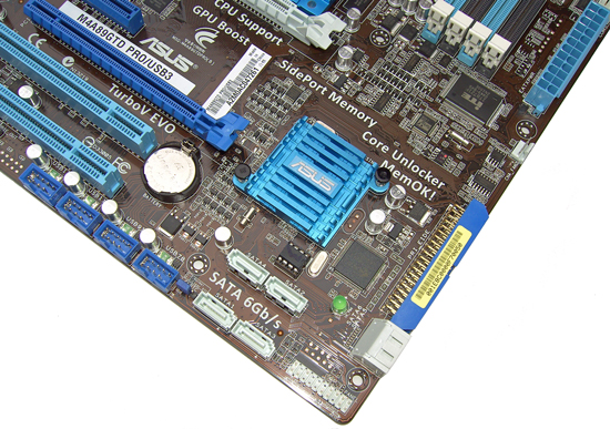
Underneath the lone DIL socket-mounted BIOS chip, four SATA ports are placed “head-on” in the bottom right corner of the board, the other two are ports right angled and situated at the bottom right hand corner. The BIOS jumper is located between the forward facing SATA ports and the USB headers. While there is the possibility of access to this jumper within a cramped PC case, we’d have preferred placement somewhere along the rear I/O panel.
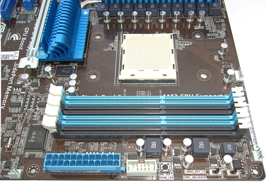
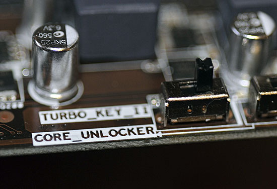
The action zone on this board is near the DIMM slots; hardware level core unlocking at the flick of a switch. To the right you’ve got a Turbo switch which applies an instant overclock much like MSI’s OC Genie.
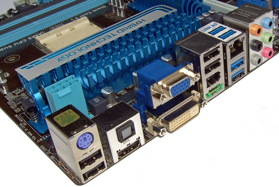
The rear I/O panel contains all audio/visual outputs, six USB ports (two are USB 3.0), 1 x RJ45, 1x eSATA, 1x 1394 and PS/2 for Keyboards.
Originally published at https://www.anandtech.com/show/2959 (Wayback Machine).