
Globalfoundries Starts on 22nm Fab & Announces First non-AMD Customer
- Posted in
- CPUs
Maintaining Moore's Law
Every two years we need the ability to make chips smaller and cram more transistors into the same area. It makes microprocessors faster, more complex and cheaper depending on what you do to them. It also really helps with the whole ridiculous pace of innovation our industry likes to maintain.
If our ability to do that came to a halt, we'd be faced with our own little economic-depression in the microprocessor industry.
The threat that it will come to a halt is real, just as the confidence that we'll be able to innovate through for the next 10 - 15 years at least. It's all a matter of size. In order to cut transistor area in half every two years, you need to be able to physically design circuits that small - which requires some very expensive and precise equipment.
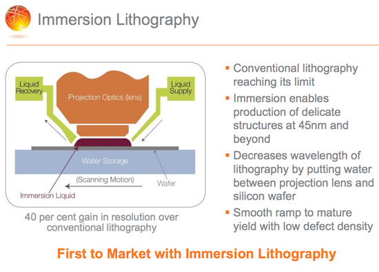
Hitting 45nm was difficult, but possible. AMD/Globalfoundries resorted to immersion lithography to make the transition. Basically it involves using liquid to improve the resolution of current 193nm lithography tools. By the time 32nm rolls around, Intel may have to do the same. Scaling beyond 32nm may reach the optical limitations of the current tools. Designing smaller, more densely packed chips may not be possible.
The replacement technology is something called extreme ultraviolet lithography. It's uses 13.5nm wavelength light (instead of 193nm) to be able to realize much finer patterns than current lithography tools.
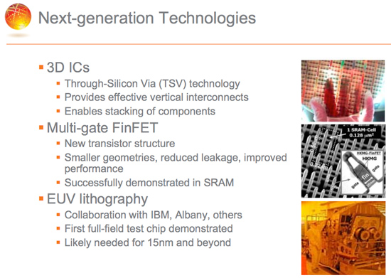
Multi-gate transistors are also expected to be needed at or after 22nm to maintain the sort of progress we've been used to. Multi-gate transistors are also non-planar so you can physically fit more in the same area, helping density issues.
Remember die-stacking? That's coming too.
Originally published at https://www.anandtech.com/show/2814 (Wayback Machine).