
Understanding the iPhone 3GS
- Posted in
- Smartphones
- Mobile
More Detail on ARM11 vs. Cortex A8
We’ve gone through the basic architectural details of the ARM11 and Cortex A8 cores, and across the board the A8 is far ahead. It gets even better for the new design once we drill a little deeper.
The L1 cache in the A8 gets a significant improvement. The ARM11 core had a 2 cycle L1 cache, while the A8 has a single cycle L1. In-order cores depend heavily on fast memory access, so an even faster L1 will have a dramatic impact on performance.
ARM11 actually supported a L2 cache but it was rarely used; the Cortex A8 is designed with a tightly coupled L2 cache varying in size. Vendors can choose from cache sizes as small as 128KB all the way up to 1MB, with a minimal access latency of 8 cycles. The L2 access time is programmable, with slower access more desirable to save power.
The caches also include way prediction to minimize the number of cache ways active when doing a cache access, this sort of cache level power management was also used by Intel back on the first Pentium M processors and is still used today in modern x86 processors.
The ARM11 core supported a 64-bit bus that connected it to the rest of the SoC; Cortex A8 allows for either a 64-bit or 128-bit bus. It’s unclear what vendors like Samsung and T.I. have implemented on their A8 based SoCs.
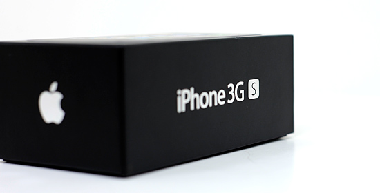
The S is for speed. Powered by the ARM Cortex A8.
With a deeper pipeline, the Cortex A8 also has a much more sophisticated branch prediction unit. While the ARM11 core had a 88% accurate branch predictor, the Cortex A8 can correctly predict branches over 95% of the time. If you care about stats, the A8 has a 512 entry branch target buffer and a 4K entry global history buffer. The accuracy of the branch predictor in the Cortex A8 is actually as high as what AMD claimed with its first Athlon processor, and this is an in-order core in a smartphone. With a 13-stage pipe however, a very accurate predictor was necessary.
While ARM11 supported some rudimentary SIMDfp instructions, Cortex A8 adds a full SIMDfp instruction set with NEON. ARM expects a greater than 2x improvement on media processing applications thanks to the A8’s NEON instructions - of course you’ll need to compile directly for NEON in order to see those gains. If you’re looking for a modern day relation, NEON is like the A8’s SSE whereas ARM11 basically had a sophisticated MMX equivalent. Both are very important.
The Cortex A8 is a more power hungry core than the ARM11, but the design also has much more extensive clock gating (turning off the clock to idle parts of the chip) than the ARM11. Since the A8 is newer it’s also going to be manufactured on a smaller manufacturing process. The bulk of ARM11 based SoCs used 90nm transistors, while A8 based SoCs are shipping at 65nm. ARM11 has started to transition down to 65nm, while A8 will move down to 45nm.
At the same clock speed and with the same L2 cache sizes, ARM shows the Cortex A8 as being able to execute 40% more instructions per second than the ARM11. That’s a generational performance improvement, something that can’t be delivered by clock speed alone, but the comparison is conservative. Cortex A8 designs won’t ship at the same clock speed and cache configurations as ARM11 chips; as far as I can tell, none of the major ARM11 based smartphones even had a L2 cache while Cortex A8 designs are expected to have one.
Furthermore, the ARM11 based smartphones were much lower in the frequency curve than the early A8 platforms. While a 40% improvement in instruction throughput is reasonable at the same specs, I would expect far larger real world performance improvements from a Cortex A8 based SoC compared to a ARM11 SoC.
Overall the Cortex A8 is much more like a modern day microprocessor. It’s still an in-order core, but it adds superscalar execution, a deeper pipeline, larger caches and a broader instruction set among other things. For any current high end smartphone there doesn’t seem to be a reason to choose the ARM11 over it, companies that insist on using ARM11 based designs even in 2009 are either not agile enough to implement a better chip in a quick manner or have no concern for performance and are more focused on cost savings. Neither option is a particularly good one and it is telling that the two manufacturers who seem to have gotten how to properly design a smartphone, Apple and Palm, have both opted to go with a Cortex A8 before most of the more established players.
A Call to Action
This leads me to a further point: we need more transparency in specs from smartphone manufacturers. The mobile phone market is all too shielded from the performance metrics and accountability that we’ve had in the PC space. When Intel was shipping Pentium 4s that performed slower than the Pentium IIIs they were replacing, we called them out on it. To this day, Apple refuses to talk about the processor in the iPhone 3GS. We get to hear all about what’s in the Nehalem Mac Pro, but the hardware behind the 3GS is off limits - despite the fact that it’s very good. This policy of not delivering specifics and a general unwillingness to talk about specs is absurd at best. It doesn’t take much more than a teardown and some homebrew code to figure out what CPU at what frequency is in any modern day smartphone; manufacturers should show pride in their hardware, or refrain from putting something inside a phone that’s they can’t be proud of.
What we need are cache sizes, clock speeds, full architecture disclosures. They don’t have to be on the phone’s marketing materials but make them accessible and at least some of the focus. These SoCs are so incredibly cool, they pack more power than the desktops of 10 years ago into a single chip smaller than my thumbnail - boast about them! Palm had a tremendous leg up on the competition with its OMAP 3430 processor, yet there was hardly any attention paid to it by Palm. I get that the vast majority of consumers don’t get, but those who do, would help tremendously if given access to this information. It’s something to get excited about.
And if the manufacturers won’t devote time and energy to this stuff, then I will.
Originally published at https://www.anandtech.com/show/2798 (Wayback Machine).