
Intel's 32nm Update: The Follow-on to Core i7 and More
- Posted in
- CPUs
Fat Pockets, Dense Cache, Bad Pun
Whenever Intel introduces a new manufacturing process the first thing we see it used on is a big chip of cache. The good ol’ SRAM test vehicle is a great way to iron out early bugs in the manufacturing process and at the end of 2007 Intel demonstrated its first 32nm SRAM test chip.
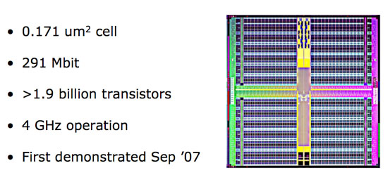
Intel's 32nm SRAM test vehicle
The 291Mbit chip was made up of over 1.9 billion transistors, switching at 4GHz, using Intel’s 32nm process. The important number to look at is the cell size, which is the physical area a single bit of cache will occupy. At 45nm that cell size was 0.346 um^2 (for desktop processors, Atom uses a slightly larger cell), compared to 0.370 um^2 for AMD’s 45nm SRAM cell size. At 32nm you can cut the area nearly in half down to 0.171 um^2 for a 6T SRAM cell. This means that in the same die area Intel can fit twice the cache, or the same amount of cache in half the area. Given that Core i7 is a fairly large chip at 263 mm^2 I’d expect Intel to take the die size savings and run with them. Perhaps with a modest increase to L3 cache size.
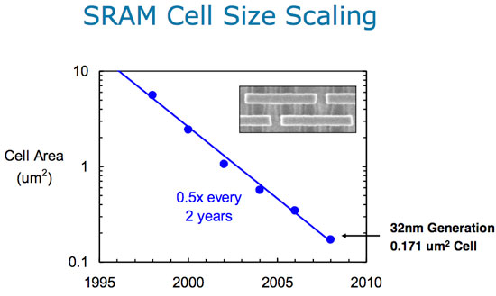
A big reason we’re even getting this disclosure today is because of how healthy the 32nm process is. Below we have a graph of defect density (number of defects in silicon per area) vs time; manufacturing can’t start until you’re at the lowest part of that graph - the tail that starts to flatten out:
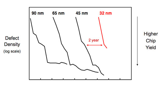
Intel’s 45nm process ramped and matured very well as you can see from the chart. The 45nm process reached lower defect densities than both 65nm and 90nm and did it faster than either process. Intel’s 32nm process is on track to outperform even that.
Two Different 32nm Processes?
With Intel now getting into the SoC business (System on a Chip), each process node will now have two derivatives - one for CPUs and one for SoCs. This started at 45nm with process P1266.8, used for Intel’s consumer electronics and Moorestown CPUs and will continue at 32nm with the P1269 process.
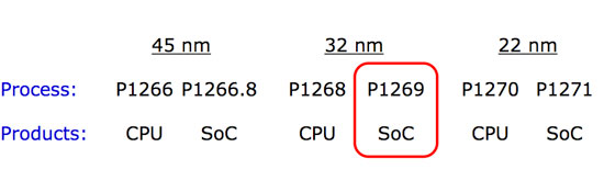
There are two major differences between the CPU and SoC versions of a given manufacturing process. One, the SoC version will be optimized for low leakage while the CPU version will be optimized for high drive current. Remember that graph comparing leakage vs. drive current of 45nm vs. 32nm? The P1268 process will exploit the arrows to the right, while P1269 will attempt to push leakage current down.
The second difference is that certain SoC circuits require higher than normal voltages and thus you need a process that can tolerate those voltages. Remember that with a SoC it’s not always just Intel IP being used, there are many third parties that will contribute to the chips that eventually make their way into smartphones and other ultra portable devices.
The buck doesn’t stop here, in two more years we’ll see the introduction of P1270, Intel’s 22nm process. But before we get there, there’s a little stop called Sandy Bridge. Let’s talk about microprocessors for a bit now shall we?
Originally published at https://www.anandtech.com/show/2722 (Wayback Machine).