
AMD Phenom II X4 940 & 920: A True Return to Competition
- Posted in
- CPUs
Phenom II's Secret, In Pictures
I can be verbose, I know, I'm sorry - I'm working on it. But on this page, I'll use pictures to illustrate my point. Here's the 65nm Phenom die:
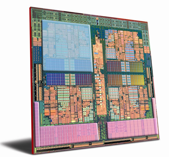
I highlighted one of the four cores in blue. The bottom part of the highlighted core its its 512KB L2 cache. The areas in pink are the 2MB L3 cache that is shared by all four cores. Now look at Phenom II:
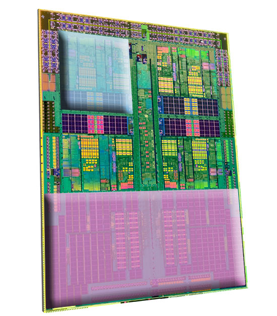
Again we've got one of the four cores highlighted blue. The L1 cache size and the core itself look very similar to the original Phenom, but note how the new die is much more rectangular. The pink area represents the Phenom II's 6MB L3 cache.
Just comparing the two die you can see that while the individual cores look similar, the amount of L3 cache has gone up considerably. Remember that Intel found with Nehalem that an 8MB L3 cache was the bare minimum, leaving 2MB per core. The original Phenom had 2MB to share amongst all four cores, which is hardly enough; Phenom II fixes that. With a 6MB L3 cache and 512KB L2 per core, Phenom II looks a lot more like Core i7 from a compute-to-cache ratio:
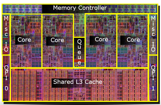
Nehalem's layout makes a little more sense, with each core butting up against the shared L3 cache, but the point is that in both Phenom II and Core i7, the L3 cache is around 1/3 of the total die. The original Phenom alloted only 1/6th of the die for its L3.
Originally published at https://www.anandtech.com/show/2702 (Wayback Machine).