
nForce 590 SLI Intel Edition: NVIDIA prepares an Intel 975X Killer
- Posted in
- CPUs
NVIDIA nForce 590 SLI: Reference Board Layout
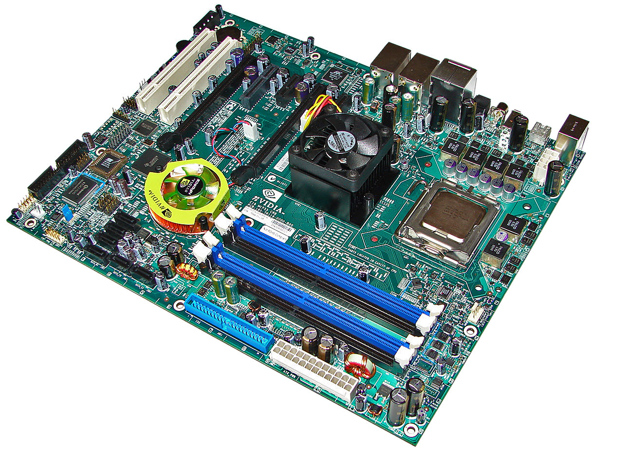
NVIDIA designed a very well laid out board with all major connections easily reached. The board is lacking most clearance issues and was very easy to install in our mid-size ATX case. The reference board features an excellent voltage regulator power design along with Rubycon and Sanyo capacitors that yielded superb stability and overclocking results even with our early BIOS and board design.
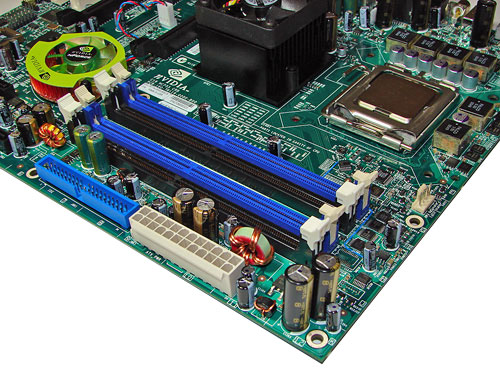
The DIMM module slots' color coordination is correct for dual channel setup based upon the premise of utilizing different colors for each memory bank. The memory modules are easy to install with a full size video card placed in the first PCI Express X16 slot. The 24-pin ATX power connector is located along the upper edge of the board along with the single IDE port connector.
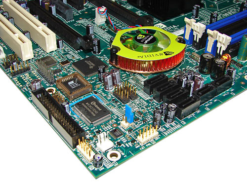
The six NVIDIA SATA ports are color coded black and are conveniently located below the NVIDIA MCP. The SATA ports feature the newer clamp and latch design. We found the positioning of the SATA ports to be excellent when utilizing either PCI-E X16 slot. The NVIDIA MCP does require a heatsink in this application.
The floppy drive connector is color coded black while being positioned along the left edge of the board. The location of this connector is not ideal and actually the whole point of having a floppy drive connector is becoming moot with the wide spread availability of USB floppy or flash drives along with BIOS support for boot purposes. The various chassis panel, USB connectors, and the second chassis fan header are located in the lower left portion of the board.
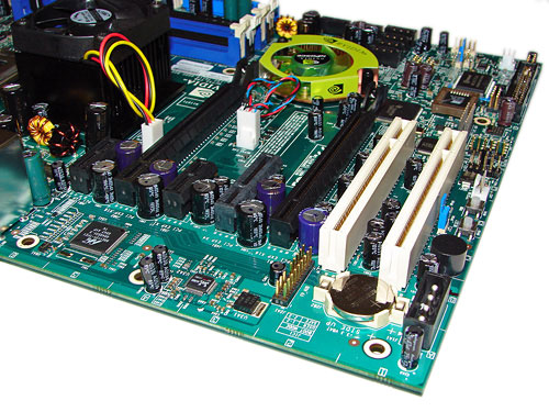
The board comes with (2) physical PCI Express X16 connectors, (1) PCI Express X1 connector, (1) PCI Express X4 connector, and (2) PCI 2.3 connectors. The layout of this design offers a very good balance of expansion slots for a mainstream board while providing excellent clearance space for graphics card utilization. Our main issue is that the first PCI 2.3 connector will be rendered physically useless if an SLI setup is utilized. Although the positioning and number of PCI-E and PCI slots are up to the manufacturer, we certainly hope to see better layouts that do not block the PCI slots in the near future. A four-pin molex power connector that is required for SLI operation and the first chassis fan header is located along the edge of the board. The four-pin molex connector is located in an unusual and difficult location to reach, the bottom left corner.
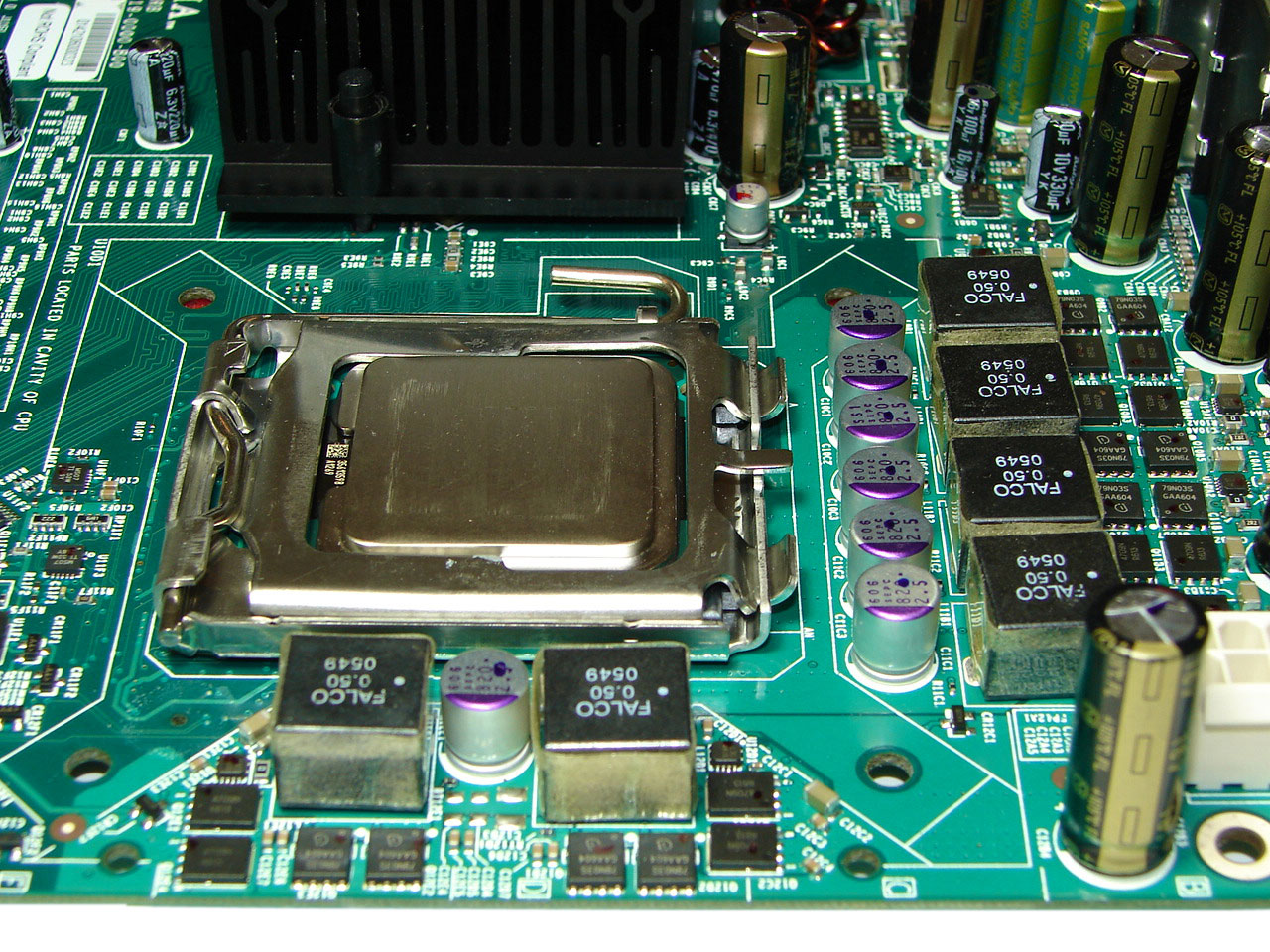
Returning to the CPU socket area, we find an ample amount of room for alternative cooling solutions. We utilized the stock heatsink/fan in our normal testing but also verified a couple of larger Socket 775 cooling solutions would fit in this area during our overclocking tests.
The NVIDIA SPP is actively cooled with a medium sized heatsink/fan unit that did not interfere with any installed peripherals. In fact this unit kept the chipset cool enough that additional chipset voltage was not a factor in our overclocking tests, although we could see this unit heating up if the HSF is not seated properly. Our only concern is the lifespan of the fan but it is very quiet during operation. NVIDIA places the 8-pin 12V auxiliary power connector at the top of the CPU socket area but out of the way of aftermarket cooling solutions.
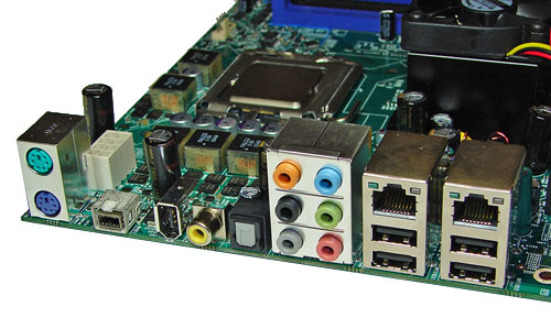
The rear panel contains the standard PS/2 mouse and keyboard ports, LAN ports, and 4 USB ports. The LAN (RJ-45) ports have two LED indicators representing activity and speed of the connection. The audio panel consists of 6 ports that can be configured for 2, 4, 6, and 8-channel audio connections. The rear panel also includes two S/PDIF (optical/coaxial) ports, an external SATA 3Gb/s port, and an IEEE 1394a port.
 |
| Click to enlarge |
NVIDIA designed a very well laid out board with all major connections easily reached. The board is lacking most clearance issues and was very easy to install in our mid-size ATX case. The reference board features an excellent voltage regulator power design along with Rubycon and Sanyo capacitors that yielded superb stability and overclocking results even with our early BIOS and board design.
The DIMM module slots' color coordination is correct for dual channel setup based upon the premise of utilizing different colors for each memory bank. The memory modules are easy to install with a full size video card placed in the first PCI Express X16 slot. The 24-pin ATX power connector is located along the upper edge of the board along with the single IDE port connector.
The six NVIDIA SATA ports are color coded black and are conveniently located below the NVIDIA MCP. The SATA ports feature the newer clamp and latch design. We found the positioning of the SATA ports to be excellent when utilizing either PCI-E X16 slot. The NVIDIA MCP does require a heatsink in this application.
The floppy drive connector is color coded black while being positioned along the left edge of the board. The location of this connector is not ideal and actually the whole point of having a floppy drive connector is becoming moot with the wide spread availability of USB floppy or flash drives along with BIOS support for boot purposes. The various chassis panel, USB connectors, and the second chassis fan header are located in the lower left portion of the board.
The board comes with (2) physical PCI Express X16 connectors, (1) PCI Express X1 connector, (1) PCI Express X4 connector, and (2) PCI 2.3 connectors. The layout of this design offers a very good balance of expansion slots for a mainstream board while providing excellent clearance space for graphics card utilization. Our main issue is that the first PCI 2.3 connector will be rendered physically useless if an SLI setup is utilized. Although the positioning and number of PCI-E and PCI slots are up to the manufacturer, we certainly hope to see better layouts that do not block the PCI slots in the near future. A four-pin molex power connector that is required for SLI operation and the first chassis fan header is located along the edge of the board. The four-pin molex connector is located in an unusual and difficult location to reach, the bottom left corner.
 |
| Click to enlarge |
Returning to the CPU socket area, we find an ample amount of room for alternative cooling solutions. We utilized the stock heatsink/fan in our normal testing but also verified a couple of larger Socket 775 cooling solutions would fit in this area during our overclocking tests.
The NVIDIA SPP is actively cooled with a medium sized heatsink/fan unit that did not interfere with any installed peripherals. In fact this unit kept the chipset cool enough that additional chipset voltage was not a factor in our overclocking tests, although we could see this unit heating up if the HSF is not seated properly. Our only concern is the lifespan of the fan but it is very quiet during operation. NVIDIA places the 8-pin 12V auxiliary power connector at the top of the CPU socket area but out of the way of aftermarket cooling solutions.
The rear panel contains the standard PS/2 mouse and keyboard ports, LAN ports, and 4 USB ports. The LAN (RJ-45) ports have two LED indicators representing activity and speed of the connection. The audio panel consists of 6 ports that can be configured for 2, 4, 6, and 8-channel audio connections. The rear panel also includes two S/PDIF (optical/coaxial) ports, an external SATA 3Gb/s port, and an IEEE 1394a port.
Originally published at https://www.anandtech.com/show/2036 (Wayback Machine).