
SUN’s UltraSparc T1 - the Next Generation Server CPUs
- Posted in
- CPUs
The 8 little cores that could
Each core is pretty small, as it has only one pipeline, no Branch Prediction Unit, no OOO buffers, and no OOO pipeline stages, which search for independent instructions. Only the large register file and thread select logic make the very simple core a bit fatter and more complex.
An 8 KB data cache and 16 KB instruction cache give an L1-hitrate of 90% or less, but it also helps to keep each core small. To keep 8 cores with such tiny L1-caches running at 70% efficiency with so many threads, a big L2-cache and massive memory bandwidth is needed.
We have quantified this effect of faster cache coherency in our Linux database server article. A dual core Opteron was about 13% faster than two single core CPUs at the same clock speed. With 8 cores that might share data, cache coherency has an even bigger impact on performance. Sharing the L2-cache also ensures that no coherency traffic is necessary on the level 2 cache.
There is more. Each core has a modular arithmetic unit (MAU) that supports modular multiplication and exponentiation to speed up Secure Sockets Layer (SSL) processing. This compensates for the lack of the FPU and the low clock speed. A single 1.2 GHz MAU seems to "sign" as fast as a 1.8 GHz Opteron, but quite a bit slower at verifying authenticity.
Each core is pretty small, as it has only one pipeline, no Branch Prediction Unit, no OOO buffers, and no OOO pipeline stages, which search for independent instructions. Only the large register file and thread select logic make the very simple core a bit fatter and more complex.
An 8 KB data cache and 16 KB instruction cache give an L1-hitrate of 90% or less, but it also helps to keep each core small. To keep 8 cores with such tiny L1-caches running at 70% efficiency with so many threads, a big L2-cache and massive memory bandwidth is needed.
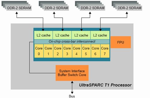
Fig 5: 8 cores fed by a 3 MB L2-cache and 4 integrated memory controllers. Source:SUN.
We have quantified this effect of faster cache coherency in our Linux database server article. A dual core Opteron was about 13% faster than two single core CPUs at the same clock speed. With 8 cores that might share data, cache coherency has an even bigger impact on performance. Sharing the L2-cache also ensures that no coherency traffic is necessary on the level 2 cache.
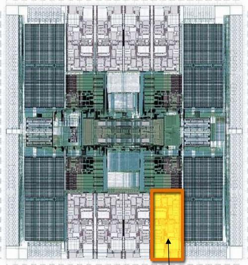
Fig 6: One (yellow) of the 8 cores (gray) of the T1. Source:SUN.
As a rough guideline, performance degrades if the number of floating-point instructions exceeds 1 percent of total instructions.Some instructions like division have long latencies, causing the thread to be skipped. The situation is then similar to a thread with a long latency load. To keep power consumption and die size per core low, each core has a very shallow six-stage pipeline: fetch, thread select, decode, execute, memory, and write back. The result is an architecture that does not need branch prediction, thanks to a shallow pipeline and FMT. However, this limits clock speed to 1.2 GHz in 90 nm, while competing chips are clocking between 2 and 4 GHz.
There is more. Each core has a modular arithmetic unit (MAU) that supports modular multiplication and exponentiation to speed up Secure Sockets Layer (SSL) processing. This compensates for the lack of the FPU and the low clock speed. A single 1.2 GHz MAU seems to "sign" as fast as a 1.8 GHz Opteron, but quite a bit slower at verifying authenticity.
Originally published at https://www.anandtech.com/show/1909 (Wayback Machine).