
NVIDIA's Scalable Link Interface: The New SLI
- Posted in
- GPUs
It's Really Not Scanline Interleaving
So, how does this thing actually work? Well, when NVIDIA was designing NV4x, they decided it would be a good idea to include a section on the chip designed specifically to communicate with another GPU in order to share rendering duties. Through a combination of this block of transistors, the connection on the video card, and a bit of software, NVIDIA is able to leverage the power of two GPUs at a time.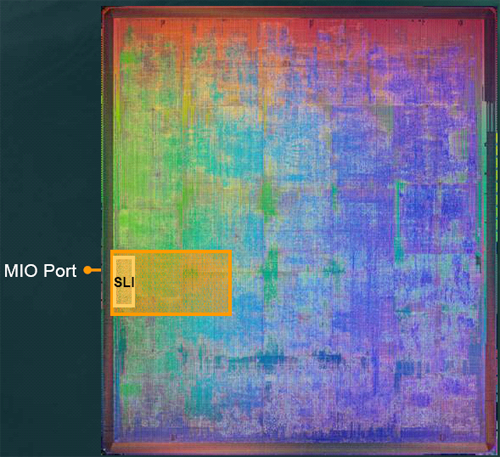
NV40 core with SLI section highlighted.
As the title of this section should indicate, NVIDIA SLI is not Scanline Interleaving. The choice of this moniker by NVIDIA is due to ownership and marketing. When they acquired 3dfx, the rights to the SLI name went along with it. In its day, SLI was very well known for combining the power of two 3d accelerators. The technology had to do with rendering even scanlines on one GPU and odd scanlines on another. The analog output of both GPUs was then combined (generally via a network of pass through cables) to produce a final signal to send to the monitor. Love it or hate it, it's a very interesting marketing choice on NVIDIA's part, and the new technology has nothing to do with its namesake. Here's what's really going on.
First, software (presumably in the driver) analyses what's going on in the scene currently being rendered and divides for the GPUs. The goal of this (patent-pending) load balancing software is to split the work 50/50 based on the amount of rendering power it will take. It might not be that each card renders 50% of the final image, but it should be that it takes each card the same amount of time to finish rendering its part of the scene (be it larger or smaller than the part the other GPU tackled). In the presentation that NVIDIA sent us, they diagramed how this might work for one frame of 3dmark's nature scene.
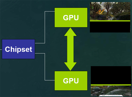
This shows one GPU rendering the majority of the less complex portion of a scene.
Since the work is split on the way from the software to the hardware, everything from geometry and vertex processing to pixel shading and anisotropic filtering is divided between the GPUs. This is a step up from the original SLI, which just split the pixel pushing power of the chips.
If you'll remember, Alienware was working on a multiple graphics card solution that, to this point, resembles what NVIDIA is doing. But rather than scan out and use pass through connections or some sort of signal combiner (as is the impression that we currently have of the Alienware solution), NVIDIA is able to send the rendered data digitally over the SLI (Scalable Link Interface) from the slave GPU to the master for compositing and final scan out.
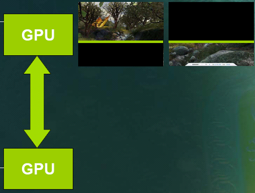
Here, the master GPU has the data from the slave for rendering.
For now, as we don't have anything to test, this is mostly academic. But unless their SLI has an extremely high bandwidth, half of a 2048x1536 scene rendered into a floating point framebuffer will be tough to handle. More normally used resolutions and pixel formats will most likely not be a problem, especially as scenes increase in complexity and rendering time (rather than the time it takes to move pixels) dominates the time it takes to get from software to the monitor. We are really anxious to get our hands on hardware and see just how it responds to these types of situations. We would also like to learn (though testing may be difficult) whether the load balancing software takes into account the time it would take to transfer data from the slave to the master.
Originally published at https://www.anandtech.com/show/1367 (Wayback Machine).