
New ATI Products Confirmed: The X Series Line-up
- Posted in
- GPUs
X300 Debuts at 110nm
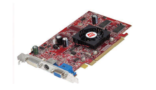
The PCI Express Radeon X300
In the same way that ATI moved into the 130nm low-k process with the 9600 line of cards, the RV370 GPU of the X300 will be fabbed on a 110nm process. As usual, TSMC is behind the silicon process that ATI is using.
It's good to see ATI sticking with a strategy that has worked for them. Taking an aggressive chance on one line of mid-range or low end GPUs before moving the rest of the parts to another process is a very good way to work out the kinks without incurring too much risk. In the worst case scenario, ATI could have covered the market segment with a lower clocked or otherwise handicapped version of a higher performing part while fixing what went wrong. What we have seen in the past with NVIDIA and large CPU vendors has consisted of large scale shifts in process technology, which can really hurt production and/or time to market if something goes wrong.
Among the benefits that ATI cites in TSMC's 110nm process is the ability to fit 40% more transistors in the same area as 130nm. A straight die shrink only accounts for about a 30% increase in space efficiency (1 - 1102 / 1302), so it stands to reason that TSMC must have made up the space savings in other areas of their process technology. Either way, this means that ATI has a lot of headroom with what they want to do with RV370.
Of course, with any new process, yeilds will be lower than what would be desired for the same performance level on an established process. Our theory is that ATI has worked out a way around this issue by taking the RV360 (Radeon 9600) core with a few tweaks, and fabbed it on a 110nm process, and dropped the clock speed way down in order to achieve acceptable yeilds. We can't be sure about this, as ATI isn't going to share yield rates or if this is actually a reason why they have taken this route. The pieces just seem to fit together too well, but it's still possible that it's all just coincidence.
The RV370 GPU will eventually be marketed as two parts: the Radeon X300 and the Radeon X300 SE. The SE part will have a cut-down 64bit memory interface similar to the 9200 SE. This value segment part will perform better than the 9200 SE part both because its based on the RV360 core, and its a higher clocked part. Hopefully, this also means that the compatibility issues we saw with the 9200 parts will fade into the distance as well. The regular X300 will have a 128bit memory interface.
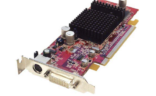
This is the half-size btx version of the X300se.
We haven't seen any of these parts yet, but if we stumble across any on the show floor at Computex, we'll be sure to include pictures.
Now, on to the mobile arena.
Originally published at https://www.anandtech.com/show/1336 (Wayback Machine).