
Samsung PC3700: DDR466 Memory for the Masses
- Posted in
- Memory
Samsung PC3700
While the JEDEC DDR standard defines both TSOP2 and BGA (Ball Grid Array) standards, most memory manufacturers produce DIMMs with TSOP2 chips.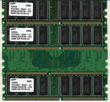
Samsung DDR466 is TSOP2 and uses the pins on each side of the memory chip for attachment to the PCB. The only high-speed BGA DIMMs that we have tested have been in our recent review Kingmax Hardcore Memory: Tiny BGA Reaches For Top Speed. Samsung supplied 4 single-sided DIMMs instead of the 2 double-sided DIMMs that we are accustomed to reviewing. However, as demonstrated in Searching for the Memory Holy Grail - Part 2, 4 single-sided DIMMs should perform at the same level as 2 double-sided DIMMs on the Intel 875 chipset used in the memory test bed.
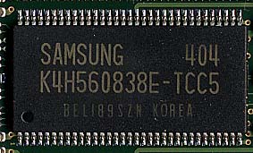
For those memory enthusiasts who want to know every detail, you can find the Samsung Part Number in the chip close-up and locate all the specs for 256Mb K4H560838E C5 chips at Samsung.
Samsung DDR466 Specifications
| Samsung DDR466 Memory Specifications | |
| Number of DIMMs & Banks | 4 DS |
| DIMM Size Total Memory |
256 Mb 1 GB |
| Rated Timings | 3-4-4-8 |
| Rated Voltage | 2.6V +/- 0.1V |
We confirmed the SPD timings to be set at 3-4-4-8. Samsung rates the C5 DDR466 chips at the same 3-4-4 timings specified for their C4 DDR400 chips. The timings and voltage specifications for DDR466 are the same as those published by JEDEC for DDR400.
The Samsung modules are rated at 2.6V +/- 0.1V, and this appears to be a very honest rating in our tests. Our highest memory overclock was achieved with 2.75V, and increasing the voltage to 2.85V did not improve stability in any way in the configuration that we were testing.
Originally published at https://www.anandtech.com/show/1269 (Wayback Machine).