
Gigabyte 7NNXP (nForce2 Ultra 400): Gigabyte Goes nForce
- Posted in
- Motherboards
Gigabyte 7NNXP: Board Layout
Overall, we were quite pleased with the 7NNXP’s layout. We like the fact that Gigabyte places the 7NNXP ATX (20-pin) connector at the top right-hand side of the PCB to the right of the DIMM slots. Since standard PSUs do not have an extra long ATX cable, this location is excellent. It will reduce clutter and greatly minimize the intrusive ATX wires from obstructing the installation/uninstallation of the CPU HSF, memory modules, and any other components that you may decide to modify or uninstall in that area. If you’re using a high-quality PSU with an extra-long ATX connector, then you have nothing to worry about, but the ATX connector location is still ideal for those users who can’t afford the best PSUs.
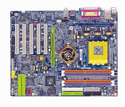
The 7NNXP’s ATX12V connector is located just below the DPS (Dual Power System), one of the 6 “Dual Miracles” that Gigabyte markets with their high-end desktop motherboards. However, it has proven to be nothing more than a marketing gimmick based on our own extensive testing. The location of the ATX12V connector is not ideal since standard PSU’s ATX12V cable runs directly over the CPU HSF. This means that you would have to unhook the ATX12V cable just to uninstall your HSF. As we’ve mentioned countless times before, this is not an issue with higher quality PSUs, but if you’re not overclocking, it seems pointless to spend extra cash on a high-watt, name-brand PSU.
For many reasons, it was wise for Gigabyte to place the Primary and Secondary IDE connectors above the midsection of the motherboard and to the right of the DIMM slots. First, this allows for bundled IDE cables to reach the upper bays of your ATX case. Secondly, it permits installation of optical drives in the first and second bays. This would not be possible if the Primary/Secondary IDE connectors were placed where the IDE RAID connectors are located on the 7NNXP. In addition, this location offers better air flow and case organization, and enables the user to make use of the Slave connector on the bundled IDE cables. All in all, you can’t go wrong with this site.
The position of the Floppy connector is less than ideal, however. In a Floppy drive installation, you’ll notice that the Floppy cable will create some case clutter and disorganization. Fortunately, the Floppy connector is right next to (and slightly above) the Primary/Secondary IDE connectors, and all the connectors will be centrally located. Still, it is not clear why Gigabyte couldn’t just place the Floppy connector at the bottom of the board near the IEEE 1394 FireWire ports.
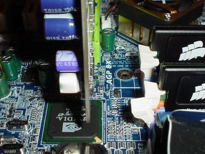
A very nice touch to the 7NNXP is the location of the DIMM connectors. They are far enough away from the AGP slot so that it doesn’t force users to uninstall their video card if they need to install or uninstall some memory. Can you imagine unscrewing your video card, unplugging your VGA cable, and physically uninstalling your video card from the AGP slot just to swap memory? Slowly, but surely, motherboard makers are taking notice of this complaint and are properly implementing the changes during layout decisions. DFI was the first of several motherboard makers to acknowledge openly that their engineers literally designed their motherboard around user requests.
Originally published at https://www.anandtech.com/show/1119 (Wayback Machine).